
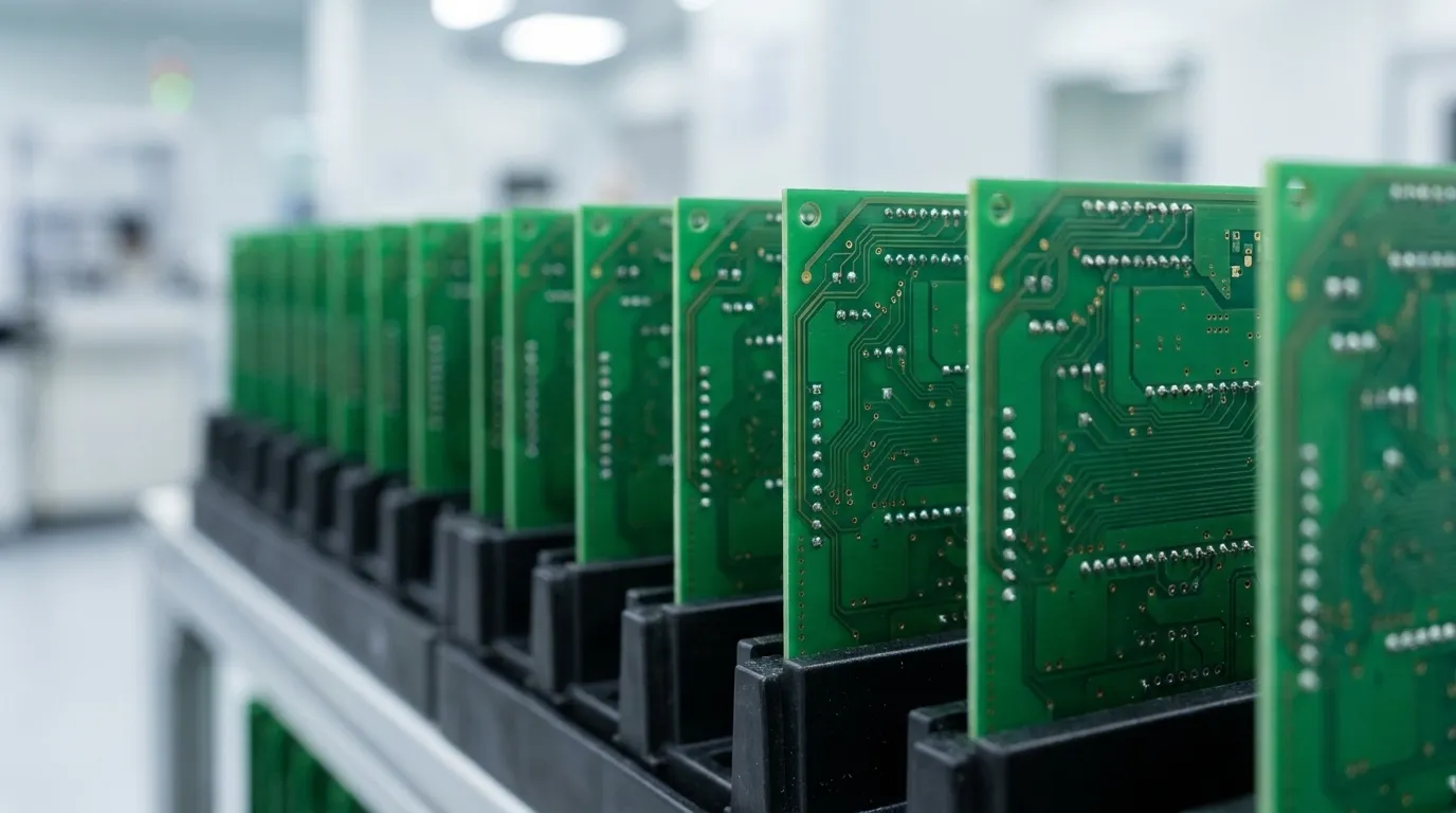
Key Takeaways for High-Temperature Flip Chip Design
- Flip-chip packaging shortens thermal paths and supports higher power densities than wire-bond alternatives in high-temperature environments.
- Material choices for interconnect alloys, underfill chemistry and substrate type directly determine long-term reliability under sustained thermal stress.
- CTE mismatch between die, substrate and board is the leading cause of warpage, bump fatigue and delamination, and early DFM review mitigates these risks.
- Integrated design-to-production workflows reduce late-stage failures because qualification results reflect actual production processes.
- Pro-Active Engineering combines thermal management expertise, advanced substrate options and certified manufacturing to deliver reliable high-temperature flip-chip solutions. Request a quote to discuss program requirements.
Temperature Bands and Mission Profiles for Flip Chip Packages
High-temperature flip-chip applications fall into three broad bands. Moderate ranges from 85 to 125°C support automotive and industrial power electronics. Elevated ranges from 125 to 175°C cover downhole tools and aerospace avionics. Extreme ranges above 175°C apply to wide-bandgap power modules and hypersonic platforms. Each band presents distinct material and process challenges.
Mission-critical programs in these bands share a common requirement. Every material and process decision made early in design directly determines field reliability. Late-stage changes carry high cost and can disqualify a program.
Direct Thermal Paths and Heat Dissipation in Flip Chip Packages
Heat removal sets the primary reliability limit in high-temperature flip-chip designs. As power density rises, conventional thermal interface materials and standard die-attach alloys restrict performance. Wide-bandgap semiconductors such as SiC support junction temperatures well above what silicon can tolerate. Realizing that capability requires a thermal path engineered to match the device.

Effective thermal path management depends on selecting materials and architectures that match power density and operating temperature. Common mitigation options include:
- Silver sintering die-attach, which offers superior thermal conductivity compared to conventional solder and measurably reduces peak die temperature versus soldered constructions
- Copper sintering, an emerging lower-cost alternative that forms a high-conductivity bond without melting the metal during processing
- Direct thermal path PCB architectures that route heat through the board stack instead of around it
- Metal-core and advanced ceramic substrates that spread heat laterally before it reaches the thermal interface
- Embedded microfluidic cooling integrated directly into the package carrier for the most demanding power densities
Pro-Active Engineering integrates silver sintering, direct thermal path technology and advanced metal-core constructions into a single design-to-production workflow. Thermal architecture decisions occur during the design phase, not after a prototype fails.
Contact the engineering team to review thermal architecture options for specific power density and operating temperature requirements.
Managing CTE Mismatch and Package Warpage
Even when thermal paths perform well, mechanical stress from thermal cycling remains a critical failure mode. Coefficient of thermal expansion mismatch between the die, substrate and board is the primary driver of warpage, bump fatigue and delamination in flip-chip assemblies. CTE mismatch causes cyclic shear stresses that fatigue solder interconnects, while adjacent-material mismatch produces warpage, delamination, misalignment and cracking. At elevated temperatures, these stresses accumulate with every thermal cycle.
CTE mismatch can be addressed at multiple levels of the package stack. At the substrate level, selecting materials whose CTE closely matches the die reduces interfacial strain at operating temperature. When organic substrates are required, symmetric layer stackups with balanced copper distribution limit residual warpage, and high-Tg or low-CTE laminates further constrain expansion. Process controls that use uniform heating, tuned cure profiles and slow cooling during lamination minimize residual stress locked into the assembly. Tailored underfill and dielectric CTE then redistribute thermal stress across the package instead of concentrating it at the bump array.
DFM review at the layout stage identifies CTE-driven risk before tooling is cut. Pro-Active Engineering uses an integrated engineering and manufacturing workflow, so the team that builds the board also reviews the stackup for warpage risk from day one.
Underfill Selection for Thermal Cycling Reliability
Underfill encapsulant mechanically couples the die to the substrate and distributes thermal stress across the bump array instead of concentrating it at individual joints. In high-temperature applications, underfill selection carries the same weight as interconnect material selection. Standard silicone gels degrade, outgas or lose dielectric strength at sustained high temperatures, so material qualification becomes a program-critical decision.
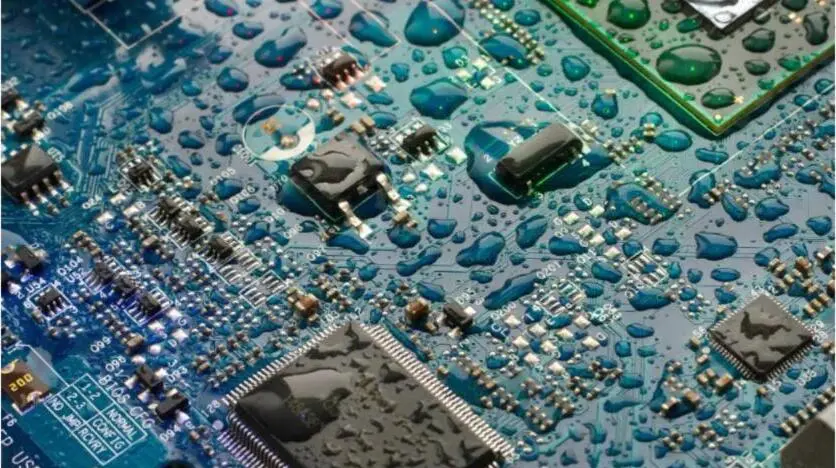
Key underfill selection considerations for high-temperature flip-chip designs include:
- Glass transition temperature relative to the maximum operating temperature of the application
- CTE compatibility with both the die and substrate to avoid new mismatch at the encapsulant interface
- Adhesion strength and resistance to delamination under repeated thermal cycling
- Filler content and particle size, which affect thermal conductivity and flow behavior during dispensing
- Compatibility with the chosen substrate surface finish and bump metallurgy
Underfill selection interacts directly with assembly process parameters. Pro-Active Engineering evaluates underfill chemistry alongside substrate and interconnect choices during the design phase, which prevents material incompatibilities from surfacing during qualification testing.
Substrate Trade-offs for High-Temperature Flip Chip Designs
Substrate selection sets the thermal, mechanical and electrical baseline for the entire package. Each substrate family involves trade-offs that must align with program requirements before layout begins.
Ceramic substrates including alumina, aluminum nitride and silicon nitride offer significantly higher thermal conductivity than organic alternatives, low CTE that closely matches semiconductor dies and dimensional stability across wide temperature swings. FR-4 under repeated thermal cycling accumulates micro-cracking in vias and solder joints, delamination between layers and gradual electrical degradation. These failure modes appear slowly and expensively over time.
Organic substrates reduce material cost and improve mechanical shock resistance but are limited by glass transition temperature and moisture sensitivity. Hybrid PCB stackups combine high-frequency laminates such as Rogers with standard FR-4 on non-critical layers to balance cost and RF/signal integrity performance for programs where full ceramic construction is not justified.
Substrate selection considerations by application tier include:
- Ceramic (AlN, Si₃N₄, Al₂O₃): preferred for sustained high-temperature operation, high power density and long service life in aerospace and defense applications
- Organic (high-Tg, low-CTE laminates): suitable for moderate temperature ranges where cost and weight constraints apply
- Hybrid: appropriate for cost-sensitive designs that require a balance of performance attributes
Discuss substrate selection trade-offs with the materials engineering team to match thermal, mechanical and cost requirements to the right substrate family for a program.
Reliability Testing and Qualification Protocols
Qualification testing confirms that a flip-chip package design survives its intended service environment. For high-temperature applications, standard commercial qualification matrices often fall short. Programs in defense, aerospace and automotive sectors require test protocols that reflect actual use conditions, including sustained elevated temperatures, rapid thermal transitions and mechanical stress.
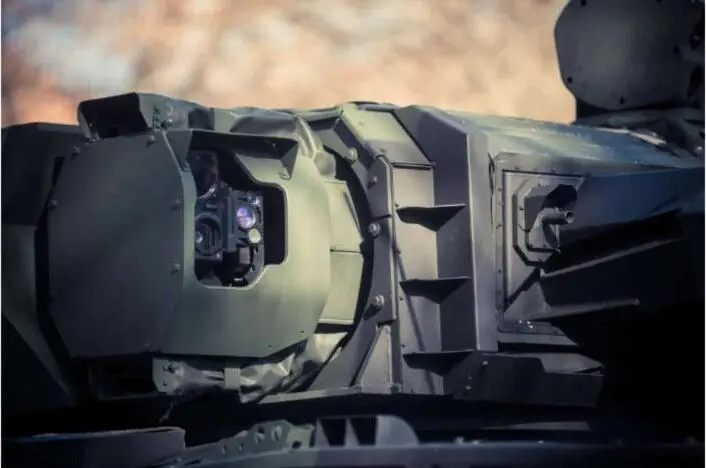
Qualification failures discovered late in a program rank among the most expensive outcomes in electronics development. The root cause often involves a mismatch between design assumptions and production reality. Power cycling data shows that interconnect and substrate material choices produce order-of-magnitude differences in cycle life, yet teams often make these choices without production input. Pro-Active Engineering uses an integrated workflow that connects design, prototyping and production under one roof, so qualification test results inform the production process directly instead of triggering a redesign loop.
Frequently Asked Questions
What interconnect materials are suitable for flip-chip packaging in high-temperature applications?
Conventional tin-silver-copper solder alloys have melting points that limit use in applications where sustained junction temperatures approach or exceed those limits. Silver sintering and copper sintering provide alternatives for high-temperature die-attach. Both form dense metallic bonds with thermal conductivity above solder and melting points far above operating temperatures, which supports reliable performance in SiC and GaN power modules and aerospace electronics. Copper sintering requires a controlled atmosphere during processing to prevent oxidation, while silver sintering is more established in production. The choice depends on cost targets, equipment availability and the specific thermal and mechanical requirements of the application.
How does CTE mismatch cause flip-chip failures, and how is it managed?
CTE mismatch occurs when adjacent materials expand and contract at different rates during thermal cycling. In flip-chip packages, this behavior generates cyclic shear stress at the bump array and at material interfaces throughout the stack. Over time, this stress produces bump fatigue, solder joint cracking, delamination between the die and substrate and warpage that affects assembly yield. As explained earlier, CTE management strategies include selecting substrate materials with CTE values close to the die, specifying underfill encapsulants that redistribute stress across the bump array, using symmetric board stackups to balance expansion forces and applying controlled lamination and cure profiles during fabrication. Early DFM review that addresses CTE compatibility before layout is finalized prevents the most costly failure modes from reaching qualification testing.
When should ceramic substrates be specified over organic substrates for flip-chip designs?
Ceramic substrates are the appropriate choice when thermal conductivity, dimensional stability and long service life under thermal cycling represent the primary requirements. Applications in aerospace, defense, automotive power electronics and industrial high-power environments typically fall into this category. Organic substrates remain viable for moderate temperature ranges where cost and weight are constrained and thermal demands remain within the laminate glass transition temperature range. Hybrid approaches, as described in the substrate section, offer a middle path for programs where full ceramic construction is cost-prohibitive but organic-only performance is insufficient. The decision should occur during the design phase, with substrate selection tied directly to the thermal model and qualification test requirements.
What qualification tests are required for high-temperature flip-chip reliability?
High-temperature flip-chip packages typically require a combination of High-Temperature Operating Life testing, thermal cycling, thermal shock, power cycling, moisture sensitivity testing and mechanical shock and vibration testing. The specific test conditions, duration and acceptance criteria depend on the application sector and the end-use environment. Defense and aerospace programs often reference military and industry standards that specify test conditions more stringent than commercial equivalents. Power cycling tests play a central role for SiC and GaN power modules because they directly measure die-attach and interconnect fatigue life under realistic operating conditions. Qualification planning should begin during the design phase so that test vehicles are built using production-representative processes, which ensures that qualification results predict field performance.
How does an integrated design-to-production workflow reduce risk in high-temperature flip-chip programs?
Fragmented vendor models, where design, prototyping and production sit with separate organizations, introduce communication gaps at each handoff. Material choices made during design may not be producible at the selected manufacturer. Prototype processes may differ from production processes, which makes qualification results less representative. Late-stage manufacturability issues discovered during production ramp also rank among the most expensive problems in electronics development. An integrated workflow closes these gaps by applying DFM from the first design review, building prototypes with the same processes and materials as production and connecting qualification test results directly to the production team. For high-temperature flip-chip programs where material and process choices are tightly coupled to reliability outcomes, this integration functions as a core risk reduction measure.
Conclusion: Reduce Program Risk with One Accountable Partner
High-temperature flip-chip packaging requires that thermal management, CTE compatibility, underfill chemistry, substrate selection and qualification testing operate as an integrated system, not a sequence of independent decisions. Each choice affects the others, and errors discovered late carry significant cost and schedule consequences.
Pro-Active Engineering consolidates PCB design, DFM, rapid prototyping through the Speed Shop, advanced interconnect and packaging, thermal management solutions and scalable production under one roof. With AS9100, ISO 9001:2015, ITAR, Nadcap and JCP certifications, the team supports mission-critical programs in defense, aerospace, automotive and industrial sectors from concept through production without the handoff risk that comes from managing multiple vendors.
For programs where flip-chip packaging reliability at elevated temperatures defines success, early engagement with an integrated partner provides a direct path to lower program risk. Request a quote to start a conversation about high-temperature flip-chip packaging requirements.