
Key Takeaways for Flip Chip Reliability
- Three dominant flip chip failure mechanisms, including solder-bump fatigue, underfill voiding and delamination, and electromigration, are preventable when addressed early in the program.
- Root causes such as bump coplanarity issues, surface contamination and current crowding are reduced through integrated DFM, material selection and disciplined process controls.
- Advanced inspection methods such as SAM, X-ray and cross-section analysis, paired with qualification testing, catch defects before late-stage qualification.
- A single engineering-led partner removes accountability gaps common in fragmented supply chains and maintains consistent control from design through production.
- Pro-Active Engineering integrates DFM, flip chip assembly, inspection and qualification testing under one roof. Request a quote to discuss program requirements.
The Problem: High-Impact Flip Chip Packaging Failures
Three dominant failure mechanisms affect flip chip packaging in production programs: solder-bump fatigue from coefficient of thermal expansion mismatch, underfill voiding and delamination, and electromigration with current crowding. Each mechanism is well understood and preventable with disciplined controls. Discovery late in qualification drives redesigns, schedule slips and compliance exposure that strain program budgets.
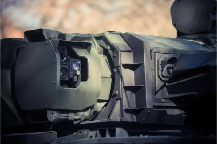
Aerospace, defense and medical programs face elevated exposure to these mechanisms. Operating environments bring wide temperature swings, sustained high-current loads and long service cycles. Fragmented supply chains that split design, assembly and inspection across multiple vendors create accountability gaps. Those gaps allow root causes to persist until qualification testing reveals them.
Solder-Bump Fatigue Driven by CTE Mismatch
Solder-bump fatigue starts with mechanical strain that builds when a silicon die and its organic or ceramic substrate expand at different rates during thermal cycling. That strain concentrates at the bump-to-pad interface. Repeated cycles initiate micro-cracks that grow until electrical continuity fails.
Several controllable factors amplify this mechanism:
- Insufficient bump-height coplanarity across the die array, which creates uneven load distribution
- Underfill material selection that fails to redistribute strain away from individual bumps
- Substrate material choices that widen the CTE difference relative to the die
- Reflow profile variation that introduces residual stress before underfill application
Pro-Active addresses these causes through DFM reviews completed before layout finalization. During these reviews, substrate material selection, bump geometry and underfill compatibility are evaluated as a single system. That integrated evaluation guides process discipline on the assembly floor, where coplanarity is controlled and reflow profiles are validated against the specific bump and substrate combination. The build then enters thermal cycling qualification with strain distribution already engineered into the design.
Underfill Voiding and Delamination in Flip Chip Builds
While solder-bump fatigue stems from CTE mismatch, a second critical failure mechanism involves the underfill material itself. Underfill redistributes thermomechanical stress across the bump array and protects the die-substrate interface from moisture and contaminants. When underfill voids or delaminates, both functions degrade. Voids concentrate stress at adjacent bumps and open paths for moisture ingress. Delamination grows under thermal cycling and can accelerate bump fatigue by orders of magnitude.
Several root causes drive underfill voiding and delamination:
- Surface contamination on the substrate or die before underfill dispense
- Surface finish selection that reduces adhesion at the underfill-substrate interface
- Dispense process variation in flow rate, temperature and cure profile that traps air beneath the die
- Chemical incompatibility between the underfill formulation and flux residue
Pro-Active manages surface preparation, surface finish selection and underfill process parameters within one controlled workflow. Inspection does not move to a downstream vendor. Scanning acoustic microscopy identifies subsurface voids and delamination before assemblies advance in the build sequence. Early detection removes the cost and schedule impact of discovering these conditions during environmental stress testing.
Defense and aerospace programs with strict reliability requirements gain predictable performance from this integrated approach. Request a quote to connect with Pro-Active’s advanced packaging team.
Electromigration and Current Crowding in Solder Bumps
Electromigration is the gradual displacement of metal atoms in a conductor driven by momentum transfer from conducting electrons. In flip chip assemblies, risk concentrates at solder bump interfaces where current density peaks. Current crowding, which is nonuniform current distribution within a bump cross-section, raises local electromigration rates and speeds void formation at the anode side of the bump.
Several design and operating factors drive electromigration risk in flip chip builds:
- Bump geometry and pitch that concentrate current at the under-bump metallization interface
- Routing topologies that funnel disproportionate current through a subset of bumps in a power delivery network
- Elevated operating temperatures that increase atomic mobility and accelerate void growth
- Insufficient bump count for the current load, which raises per-bump current density
Pro-Active’s engineering team evaluates current distribution during the DFM phase. The team reviews power delivery routing, bump count and under-bump metallization stack selection against the thermal and electrical load profile of the application. On the production floor, process controls maintain bump geometry and reflow conditions consistent with the design analysis. Qualification testing, including accelerated life testing under representative current and temperature conditions, then confirms that the as-built assembly performs within the intended design envelope.
Inspection Methods That Catch Flip Chip Failures Early
Inspection complements process control and provides direct evidence of build quality. Three methods deliver meaningful coverage for flip chip failure mechanisms: scanning acoustic microscopy, X-ray imaging and cross-section analysis.
- Scanning acoustic microscopy (SAM): Detects subsurface voids, delamination and disbonds in the underfill and at the die-substrate interface without destroying the assembly. SAM serves as the primary tool for underfill quality verification.
- X-ray imaging: Reveals bump coplanarity issues, bridging and gross voiding within the solder bump array. Two-dimensional and three-dimensional X-ray provide complementary views of bump integrity across the full array.
- Cross-section analysis: Provides direct metallographic evidence of crack initiation, void formation and intermetallic compound growth at bump interfaces. This method supports failure analysis and process validation.
Pro-Active integrates these inspection methods into its quality system as part of a closed-loop process. Inspection data feeds back into process control decisions and guides adjustments on the assembly floor.
Qualification Testing Flow for Production Confidence
Qualification testing confirms that a flip chip assembly performs reliably under its intended operating conditions. Pro-Active executes a structured qualification flow with the following stages:
- Pre-stress baseline inspection: SAM, X-ray and electrical characterization establish the as-built condition before stress application.
- Thermal cycling: Assemblies undergo repeated temperature excursions that represent the application environment to assess bump fatigue and underfill integrity.
- Thermal shock: Rapid transitions between temperature extremes expose weaknesses in bump and underfill adhesion that gradual cycling may not reveal.
- Highly accelerated stress testing (HAST) or moisture sensitivity testing: Evaluates resistance to moisture ingress at the underfill-substrate interface.
- Electromigration testing: Confirms bump current-carrying capacity under elevated temperature and current conditions that represent worst-case operation.
- Post-stress inspection and failure analysis: SAM, X-ray and cross-section analysis confirm pass or fail status and identify any degradation mechanisms for process feedback.
Executing this flow in-house with the same engineering team that performed DFM and managed assembly keeps every finding immediately actionable. No handoff delay occurs between the test lab and the process engineer.
FAQ: Engineering-Led Manufacturing and Compliance
How does an engineering-led manufacturer reduce the risk of discovering packaging issues during qualification?
An engineering-led manufacturer embeds failure-mode knowledge into design and process planning rather than relying on qualification testing to uncover problems. When DFM, material selection, process control and inspection remain under one team, early decisions account for the thermal, electrical and mechanical conditions present in qualification. Issues that might appear as qualification failures are identified and resolved before the first build completes. Pro-Active’s integrated workflow connects design engineers and manufacturing engineers from the initial review through production release, which compresses the feedback loop and reduces late-stage surprises.
What traceability and compliance advantages does a domestic ITAR-registered provider offer for regulated programs?
A domestic ITAR-registered manufacturer operates under regulatory obligations that govern data handling, personnel access and documentation practices. For defense and aerospace programs, controlled technical data associated with the assembly, including design files, process records and inspection data, remains within a compliant environment throughout the program lifecycle. Pro-Active maintains ITAR registration, AS9100 certification, JCP certification and Nadcap accreditation. Full traceability documentation is generated and retained for every build to support program audits, failure investigations and lifecycle management.

How does Pro-Active support the transition from prototype to production while maintaining the same process controls?
Pro-Active’s rapid prototyping capability, the Speed Shop, uses the same production processes, equipment and quality controls as full-volume builds. Process parameters validated during prototype qualification carry directly into production. No requalification is required when a program scales because the process baseline remains consistent between prototype and production. Engineering and manufacturing operate within one workflow, so DFM decisions, material selections and inspection criteria established during development continue without translation loss across vendor boundaries.
Why is working with a single accountable partner preferable to managing multiple vendors for flip chip assembly?
Fragmented supply chains distribute accountability across vendors and complicate root cause identification. When design, assembly, underfill processing and inspection occur at separate organizations, each vendor focuses on its own scope. Interface conditions such as surface preparation before underfill, reflow profile compatibility with bump geometry and inspection criteria aligned to design intent can fall into gaps between scopes. A single accountable partner owns those interfaces. Pro-Active manages DFM, flip chip assembly, advanced inspection and qualification testing under one roof, so process adjustments are decided and implemented by the same team without multi-vendor coordination cycles.
Conclusion: Integrated Control for Reliable Flip Chip Programs
The three failure mechanisms discussed are well characterized and respond to disciplined process controls applied from design through qualification. Organizational structure determines whether those controls reach every build. Integrated capability under one roof removes the accountability gaps common in multi-vendor workflows and supports consistent reliability.
Pro-Active Engineering provides flip chip assembly, advanced interconnect and full qualification support from its 45,000-square-foot facility in Sun Prairie, Wisconsin. The company operates as a certified, ITAR-registered domestic manufacturer serving aerospace, defense and medical programs.
Request a quote to start a conversation about flip chip assembly and advanced packaging with Pro-Active Engineering’s team.