

Last updated: July 29, 2026
Key DFM Lessons for Reliable PCB Assembly
- A structured DFM checklist for PCB assembly reliability links each design decision to known defect modes, IPC standards and inspection methods before fabrication.
- Core checklist items address component orientation, pad and solder-mask design, via placement, thermal relief, footprint validation, testability and documentation.
- Early DFM review during schematic capture and layout prevents tombstoning, bridging, BGA voiding and placement errors that otherwise surface during assembly.
- Scaling from prototype to volume production without losing reliability requires an integrated workflow that removes handoff gaps between design, prototyping and assembly.
- Pro-Active Engineering delivers this integrated workflow under one roof; begin a DFM review on the next program.
Core DFM Checklist for PCB Assembly Reliability
Pro-Active Engineering applies a structured set of design rules before fabrication and assembly begin. Each rule maps to a known defect mode and inspection method. The review sits inside a single integrated workflow from initial layout through production, so issues are resolved at the design stage rather than on the assembly floor.
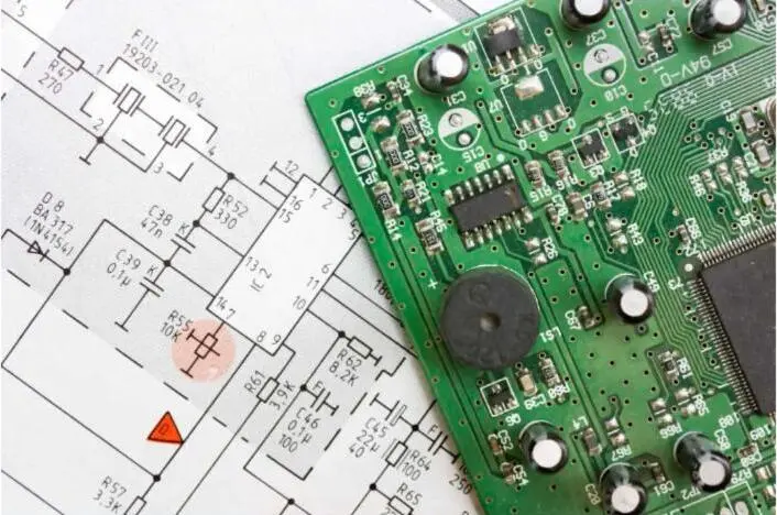
Component Placement and Orientation for Stable Reflow
Consistent component orientation reduces tombstoning and placement error rates during reflow. Polarized passives and fine-pitch ICs respond differently to heat and conveyor motion when orientation varies across the board. Standardized orientation keeps thermal and mechanical forces predictable during soldering.

- Orient all passive components and SOICs so solder lands run perpendicular to the direction of board travel on reflow and wave-solder conveyors.
- Maintain consistent pin-1 orientation for all ICs across the board.
- Keep component bodies separated by adequate clearance.
- For Class 3 assemblies, IPC-A-610 maintains strict criteria for the alignment and orientation of polarized components.
Pad and Solder-Mask Design for Bridging Control
Solder-mask dams are thin strips of protective coating that separate adjacent pads on fine-pitch components. These dams block solder from flowing between pads during reflow. Missing or insufficient solder-mask dams sharply increase bridging risk because solder can move without a physical barrier. Pad geometry and mask openings must be validated together to maintain adequate dam width.
- Maintain a minimum solder-mask dam between adjacent pads on fine-pitch components.
- Apply symmetric pad geometry for all passive components.
- Use a windowpane or crosshatch stencil aperture pattern over QFN thermal pads.
- Keep silkscreen ink clear of BGA pads.
Via and Copper Rules for Robust Interconnects
Via-related defects commonly arise from mismatched hole size versus board thickness, incorrect via placement on pads and insufficient clearance between vias and conductors. Mismatched hole sizes compromise plating uniformity, vias on pads create solder-wicking paths that starve joints and inadequate clearance increases the risk of shorts. Together, these failures reduce plating quality, solder reliability and long-term durability.
- Maintain the minimum annular ring on all vias.
- Fill and cap all vias placed in BGA or QFN pads.
- Enforce adequate via-to-copper clearance.
- Keep vias a minimum distance from component lands and connect them with a narrow surface conductor.
Thermal Relief and High-Power Layout Practices
Thermal dissipation becomes a primary failure mode as component density and power levels increase. Local hot spots and coupled thermal paths can damage components and degrade solder joints. Thermal analysis during design identifies these risks so layout and copper features can spread heat effectively.
- Apply thermal relief spokes to all through-hole pads connected to copper planes.
- Balance copper distribution symmetrically across the layer stack.
- Integrate thermal simulation before layout is finalized on high-power designs. Pro-Active Engineering’s thermal management capabilities address these requirements at the design stage.
- Verify that high-current paths carry adequate trace width and copper weight.
Footprint Validation and IPC-7351 Alignment
IPC-7351 provides a formula for calculating land pattern dimensions and defines three standard density levels for component footprints. These standards align pad sizes with component geometry and assembly tolerances. Correct alignment improves manufacturability and yield across different board densities.
- Select the IPC-7351 density level (A, B or C) appropriate for the program.
- Validate BGA pad size against ball diameter and pitch.
- Confirm footprint-to-BOM alignment before release.
- Cross-check all land patterns against the manufacturer’s datasheet dimensions.
Testability and Panelization for Reliable Inspection
PCB test strategy should be reviewed early, before layout begins, with manufacturing teams involved to identify Design for Test risks. Testability describes how easily a board can be verified through automated inspection and electrical testing. Features such as test points, fiducials and debug interfaces built into the design prevent coverage gaps that only appear during production.
- Add dedicated test points on power rails, ground, critical signals and communication buses to enable ICT and flying-probe access.
- Include at least three global fiducials and local fiducials for each fine-pitch component.
- Design panelization with V-scores or routed tabs, tooling holes and adequate rail width for conveyor support.
- Include debug interfaces such as JTAG, SWD or UART headers and label critical signals on silkscreen.
BOM and Documentation Requirements for Smooth Release
Locking the BOM, resolving end-of-life component risks and establishing approved alternate MPNs are essential steps before committing to production. Failing to complete these steps creates documentation gaps such as missing alternates, unresolved EOL parts or BOM inconsistencies. These gaps cause delays that exceed the time required to resolve them during design.
- Scrub the BOM for EOL and NRND parts before design release. Pro-Active Engineering uses SiliconExpert for BOM scrubbing and lifecycle risk mitigation.
- Consolidate component values to reduce unique line items and machine setup time.
- Apply counterfeit avoidance methodology per SAE AS5553B. Pro-Active Engineering’s sourcing process aligns to this standard to prevent counterfeit components from entering the supply chain.
- Prepare a complete documentation package including fabrication drawings, assembly drawings, a full BOM with manufacturer part numbers and packages and a readme covering special requirements.
Pre-Release Reliability Review as Final Gate
A thorough DFM review catches most production issues before a single board is built, turning the checklist items above into a final gate before fabrication release. This review confirms that design intent, process capability and quality expectations align before production funds are committed.
- Confirm IPC-A-610 class designation is documented and agreed upon before sign-off.
- Verify that the soldering process and materials comply with J-STD-001.
- Confirm that X-ray inspection is planned for all BGA and bottom-terminated components.
- Validate that the stack-up, copper balance and material selection are frozen before fabrication.
Scaling from Prototype to Volume Without Losing Reliability
Industry data indicates that a large share of PCB assembly defects originate from poor PCB design. A structured DFM review prevents many common assembly defects and increases first-pass yield. Completing these pre-release checks addresses design-stage risks, but maintaining that discipline as builds scale from prototype to production introduces a different challenge.
Pro-Active Engineering addresses this through a single integrated workflow in Sun Prairie, Wisconsin, where design, rapid prototyping, PCB assembly, conformal coating, testing and box build operate in sequence without vendor handoffs. The Speed Shop delivers production-ready prototypes using the same processes as full-scale builds, so what works at prototype scale transfers directly to volume production without process translation risk.

For aerospace, defense and medical device manufacturing, the transition to production must be handled by an ITAR-registered, AS9100-certified facility supporting IPC-A-610 Class 3 build standards. Pro-Active Engineering holds ISO 9001:2015, AS9100 and Nadcap accreditation, is ITAR-registered and JCP-certified and aligns to NIST 800-171 with CMMC readiness. Full traceability and documentation control are standard on every program, not optional add-ons.

DFM functions as a continuous discipline at Pro-Active Engineering rather than a single gate at the end of design. Engineering and manufacturing operate within one workflow, so manufacturability, sourcing insight and quality planning are integrated from day one. That structure eliminates the prototype-to-production disconnect that causes late-stage defects, redesigns and cost overruns in fragmented supply chains.
Connect with Pro-Active Engineering’s team to begin a DFM review on an active program.
Download the Complete DFM Checklist
The checklist items in this guide are available as a printable reference. Engineering teams working on Class 2 or Class 3 programs can use it as a pre-release validation tool before submitting design packages for fabrication and assembly. Pro-Active Engineering shares the complete checklist and explains how the integrated workflow applies to a specific program.
Get the full checklist and schedule a DFM consultation with Pro-Active Engineering’s engineering team.
Frequently Asked Questions
What is the difference between a bare-board DFM review and a PCBA DFM review?
A bare-board DFM review focuses on fabrication constraints such as layer stackup, drill sizes, trace widths, copper balance and material selection. A PCBA DFM review extends that scope to assembly processes, covering component placement, pad geometry, solder-mask dams, via-in-pad treatment, stencil apertures, panelization, fiducials and test access. Both reviews are necessary for high-reliability programs. Skipping the PCBA review leaves a significant category of defect risk unaddressed, including tombstoning, solder bridging, BGA voiding and placement registration errors that only surface during assembly.
When in the design process should a DFM review happen?
DFM review is most effective when it begins during schematic capture and continues through layout. Reviewing a completed layout before fabrication release catches many issues, but some problems such as component selection that creates footprint mismatches or thermal management gaps are easier and less costly to resolve earlier. Pro-Active Engineering integrates DFM into the design phase as part of its engineering workflow, so manufacturability is evaluated continuously rather than as a single gate before tape-out.
How does IPC-A-610 Class 3 differ from Class 2 in practice?
IPC-A-610 Class 2 applies to dedicated-service products where continued performance is required but uninterrupted service is not critical. Class 3 applies to high-performance products where failure is unacceptable, including electronics used in defense, aerospace and implantable medical applications. In practice, Class 3 imposes tighter solder fillet minimums, stricter surface condition tolerances, more rigorous documentation requirements and zero tolerance for conditions that Class 2 would accept as marginal. Inspection criteria, operator certification requirements and traceability expectations all increase under Class 3. Pro-Active Engineering builds to IPC-A-610 Class 2 standards.
What makes an integrated EMS partner preferable to separate design and assembly vendors for high-reliability programs?
Vendor fragmentation introduces handoff gaps between design, prototyping, assembly, coating and test. Each gap creates opportunities for information loss, misinterpretation of design intent and accountability disputes when defects surface. For defense, aerospace and medical programs operating under strict compliance and traceability requirements, those gaps translate into program risk. An integrated partner maintains a single chain of custody from design through box build with one quality management system, one documentation package and one point of accountability. Pro-Active Engineering consolidates all of these services under one roof, which reduces coordination overhead and lowers the risk of late-stage manufacturability surprises.
How does Pro-Active Engineering support traceability requirements for regulated industries?
Pro-Active Engineering’s quality management systems and certifications, detailed in the scaling section above, support full traceability and documentation control as part of the standard production workflow, not as optional add-ons. Every program includes traceability documentation. Pro-Active Engineering uses SiliconExpert for BOM scrubbing and lifecycle risk mitigation and aligns its sourcing process to SAE AS5553B for counterfeit avoidance. For programs with CMMC or NIST 800-171 requirements, Pro-Active Engineering maintains alignment to those frameworks as part of its standard operating environment.