
Key Takeaways
-
Device type (Si, SiC, GaN, IGBT) and substrate (DBC, AMB, copper, AlN) determine die attach process selection for power electronics.
-
Silver sintering delivers strong thermal conductivity and high-temperature stability for SiC and high-power IGBT modules in demanding applications.
-
Eutectic AuSn/AuSi bonding supports hermetic, load-bearing and high-reliability builds where organic materials are prohibited or traceability standards are strict.
-
Solder die attach fits lower-temperature, cost-sensitive or high-volume designs where junction temperatures stay within solder limits.
-
Pro-Active Engineering offers all three processes under one roof with full inspection, traceability and compliance credentials, and supports power electronics programs from prototype through production. Request a quote to start a power electronics program.
Die Attach Services For Power Electronics
Die attach services for power electronics are contract manufacturing processes that bond semiconductor dies such as silicon, SiC, GaN or IGBT to substrates such as DBC, AMB, copper or AlN using silver sintering, eutectic AuSn/AuSi bonding or solder. The choice depends on device type, substrate, thermal budget and reliability requirements.
Matching the process to the device and substrate forms the foundation of every power electronics build. Request a Die Attach Consultation to review options for a specific program.
The Problem: Why Process Selection Determines Power Electronics Reliability
Selecting the wrong die attach method produces predictable failure modes. Thermal fatigue accumulates at the bond interface under repeated power cycling, and voiding reduces the effective thermal conductance that would otherwise carry heat away from that interface. The resulting hot spots concentrate mechanical stress, which speeds intermetallic growth and degrades joint integrity. In high-current, high-temperature applications, these failure modes feed each other.
The deeper problem is structural. A manufacturer running only one die attach process will recommend that process regardless of device and substrate needs. A device-and-substrate-driven selection framework applied by a partner with multi-process capability aligns process choice with program requirements and supports domestic execution with full compliance documentation.
Silver Sintering Die Attach For SiC And IGBT
Silver sintering has become a leading die attach process for SiC and IGBT power devices. Silver sintering offers thermal and electrical conductivity that solder cannot match, and the finished joint tolerates operating temperatures that would soften a solder joint. Because the bond forms below silver’s melting point, the joint avoids the intermetallic aging that eventually degrades solder. This behavior supports power devices that run hot continuously.

Materials suppliers including Heraeus, Indium Corporation and MacDermid Alpha supply qualified silver sinter pastes for power module applications. Pro-Active Engineering offers silver sintering as part of its advanced interconnect and thermal management capabilities.
Silver Sintering Vs. Solder Die Attach For SiC Power Modules
For SiC applications, silver sintering provides stability at continuous temperatures above what lead-free solders can sustain. The silver joint does not undergo the phase transitions that cause fatigue and degradation in solder alloys. Solder remains viable for lower-temperature SiC designs where junction temperature stays within solder operational limits and cycle life requirements are less demanding.
Pressure Vs. Pressureless Silver Sintering In Production
Pressure-assisted sintering applies a defined load during the cure cycle. Applied pressure forces trapped gases outward before nanoparticles fuse, which increases contact area beneath high-power chips and typically lowers voiding. The tradeoff is specialized tooling, handling fixtures and tighter process controls. These requirements fit demanding aerospace and defense programs more than high-volume commodity production.
Pressureless sintering eliminates the pressurization step and the associated equipment investment. Pressureless sintering can directly replace existing high-lead soft solder without additional equipment investment, which supports continuous automated production. It tightens requirements on paste formulation, atmosphere control and thermal uniformity to achieve comparable joint quality. Once tier-1 module makers validate pressureless silver sintering on standard production equipment, qualification cycles compress from years to months.
Eutectic Die Attach (AuSn/AuSi) For High-Reliability Power
Eutectic bonding is recommended when the thermal path is load-bearing, the package must seal hermetically or no organic material is permitted inside the cavity. Sealing a polymer inside a hermetic cavity causes it to release volatiles over the life of the part, which disqualifies epoxy die attach in hermetic or optical builds regardless of thermal performance.
Eutectic bonding retains advantages over sintering in specific contexts. It has an established reliability heritage traceable through IPC-9701B thermal cycling qualification and MIL-STD-883 Method 2019 die shear testing. It is compatible with certain substrate metallizations and suits lower-volume, high-mix programs. Gold-based materials and the process control they require increase per-unit cost. Eutectic bonding may not scale as economically as sintering for high-volume SiC modules.
Eutectic AuSn Vs. AuSi Die Attach For High-Reliability Power
AuSn 80/20 reflows at a single temperature with a sharp solid-to-liquid transition, which makes it the workhorse for step-soldering and hermetic builds. Its process temperature is compatible with packages that contain organic materials. AuSi offers higher thermal conductivity than AuSn but requires a process temperature that is incompatible with any package containing plastic. Package construction, thermal path requirements and the presence of organic materials guide the choice between them.
Solder Die Attach For Cost-Sensitive Power Designs
Solder die attach remains appropriate for lower-temperature, cost-sensitive and high-volume power applications where sintering or eutectic bonding is not required by the device or substrate. For Si devices operating within conventional junction temperature limits, and for IGBT modules at standard power densities, solder provides a technically adequate and economically practical attach method.
The same failure modes described earlier, thermal fatigue, voiding and intermetallic growth, apply here with one distinction. Sintered silver avoids the phase transitions that drive these mechanisms in solder. Lead-free solders such as SAC305 are limited to lower continuous operating temperatures, which makes them unsuitable for SiC devices that routinely operate above those limits.
Die Attach For GaN Transistors: Why Thermal Resistance Dominates
GaN’s higher current density is confined to a small region around the GaN/AlGaN heterojunction interface, which makes thermal management more demanding than the bulk thermal conductivity figure alone suggests. Because GaN devices use a lateral structure confined to the top of the die, much of the cooling benefit available to vertical Si and SiC devices bonded directly to a copper lead frame is reduced in legacy packages. Silver sintering or advanced solder systems are relevant for GaN die attach because minimizing thermal resistance at the bond interface is the dominant design constraint. That same device-first logic applies across all power technologies, which is why the selection guide below starts with the device and substrate rather than the process.
Device And Substrate Selection Guide
The mapping below shows how device type and substrate narrow the process choice before thermal budget, reliability requirements and production volume refine it. Read it as a decision sequence that starts with the device, then the substrate, then the program constraints.
By device type:
-
Silicon (Si): Solder die attach is typically adequate for conventional power densities and junction temperatures within standard limits. Silver sintering or eutectic bonding applies when reliability requirements or operating conditions exceed what solder can sustain.
-
SiC: Silver sintering is the emerging standard for SiC power devices in applications where junction temperatures exceed the practical service limit of solder. Eutectic bonding applies in low-volume or hermetic SiC builds. Solder remains viable only where junction temperature stays within solder operational limits.
-
GaN: Silver sintering or advanced solder systems are preferred. Thermal resistance at the bond interface is the dominant selection criterion given GaN lateral structure and confined current density.
-
IGBT: Solder is cost-effective and technically adequate at standard power densities. Silver sintering fits high-power-density IGBT modules where junction temperature and cycle life requirements exceed solder capability.
By substrate type:
-
DBC (Direct Bonded Copper): Compatible with solder and silver sintering. DBC on alumina is cost-effective for conventional power circuits but has CTE mismatch limitations under severe thermal cycling. Silver sintering is preferred on DBC/AlN for SiC applications.
-
AMB (Active Metal Brazing): AMB on Si₃N₄ provides the closest CTE match to SiC among industrially available ceramics, which makes it the substrate of choice for severe thermal cycling applications. Silver sintering is the preferred die attach for AMB/Si₃N₄ combinations in traction and high-reliability programs.
-
Copper: Compatible with solder and silver sintering. Surface metallization must be verified for sintering compatibility. Silver or gold surface finish supports reliable sinter bonding.
-
AlN: AlN CTE is nearly identical to silicon and close to GaN, which makes it preferable for direct die attach in power semiconductor modules. It is compatible with silver sintering, eutectic bonding and solder. Device type and thermal budget drive the final process choice.
What To Demand From A US Die Attach Contract Manufacturer
Process and substrate selection deliver results only when the manufacturer can execute them. Evaluating a US die attach contract manufacturer for power electronics programs therefore requires verifying capability across five areas.
-
Sintering capability: A manufacturer that runs only one sintering variant will steer every program toward it, which reintroduces selection bias. Running both pressure-assisted and pressureless sintering keeps the process choice tied to the device and substrate.
-
Void inspection capability: Visual inspection cannot detect subsurface voids. X-ray at multiple angles and scanning acoustic microscopy (SAM) are the production-standard non-destructive methods. The manufacturer should provide void inspection data with traceability to the reflow profile and substrate lot.
-
Substrate handling expertise: DBC, AMB, copper and AlN substrates each have distinct handling, metallization and thermal mass requirements. The manufacturer must demonstrate experience with the specific substrate the program requires.
-
Qualification documentation: Programs requiring AS9100 or Nadcap-level documentation need a partner whose quality system produces traceable records at every process step.
-
Domestic compliance: ITAR registration is commonly required for defense and aerospace programs. Domestic manufacturing reduces IP risk and logistics exposure compared with offshore production.
Pro-Active Engineering runs all three processes under one roof, which allows the device-and-substrate framework described above to drive the recommendation. Advanced interconnect capabilities including wire bonding, flip chip and hybrid assemblies integrate with die attach in a single workflow. Thermal management solutions including direct thermal path technology and metal-core constructions support high-power program requirements. Founded in 1996 and located in Sun Prairie, Wisconsin, Pro-Active holds ISO 9001:2015 and AS9100 certifications, is ITAR registered and Nadcap accredited and carries CAGE code 7R4Q2.
What To Ask A US Die Attach Contract Manufacturer
-
Can the line run both pressure-assisted and pressureless silver sintering?
-
What void inspection methods are used, X-ray, SAM or both, and at what inspection frequency?
-
How are DBC, AMB, copper and AlN substrates handled and fixtured through the process?
-
What qualification documentation is provided, and how is traceability maintained to substrate lot and reflow profile?
-
Is the facility ITAR registered, AS9100 certified and Nadcap accredited?
Request a Quote for Die Attach Services
Prototype-To-Production Reality
Once a manufacturer clears those criteria, the next step is de-risking the program before volume commitment. Validating the die attach process on a prototype build provides that proof. A small prototype build using the target process, substrate and device combination, followed by void inspection and thermal performance verification, reduces program risk before scaling.
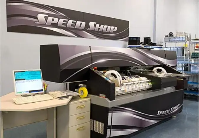
Pro-Active Engineering Speed Shop builds prototypes on the same sintering, eutectic or solder lines that will run at volume. Because the process does not change between prototype and production, the manufacturability failures that appear when a program switches processes or partners stay out of the program. The integrated workflow carries the validated process straight into production release.
Frequently Asked Questions
What Is The Best Die Attach Process For SiC Power Devices?
Silver sintering is the preferred process for most SiC power device applications. It provides thermal conductivity and high-temperature stability that solder cannot match at the junction temperatures SiC devices routinely sustain. Eutectic bonding applies in hermetic or low-volume SiC builds where gold-based metallurgy is required. Solder remains viable only for SiC designs where junction temperature stays within solder operational limits and cycle life requirements are less demanding.
Can Solder Die Attach Be Used For GaN?
Solder die attach is possible for GaN, and GaN lateral structure and confined current density make thermal resistance at the bond interface the dominant reliability constraint. Advanced solder systems or silver sintering are typically preferred when junction temperature and long-term reliability requirements drive the design.
What Should A Buyer Look For In A US Die Attach Contract Manufacturer?
The five criteria are covered in the manufacturer evaluation section above. The short version: multi-process capability, void inspection, substrate handling, qualification documentation and domestic compliance credentials.
Does Pro-Active Engineering Offer Silver Sintering And Eutectic Die Attach?
Pro-Active Engineering runs silver sintering, eutectic bonding and solder die attach under one roof. Advanced interconnect capabilities including wire bonding, flip chip and hybrid assemblies are integrated into the same workflow, which supports complete power electronics packaging programs from prototype through production.
About The Manufacturer
Pro-Active Engineering operates a 45,000 sq. ft. facility in Sun Prairie, Wisconsin, with a workforce of more than 120 electronics professionals. The certifications and registrations listed earlier apply across all services. PCB design, rapid prototyping, advanced die attach, interconnect and system integration are executed under one roof.
Conclusion
Die attach process selection for power electronics is determined by device type and substrate. Silver sintering, eutectic bonding and solder each serve a defined role in that decision framework. A US contract manufacturer should run all three, provide void inspection data with full traceability and deliver the compliance documentation that defense, aerospace and industrial programs require. Pro-Active Engineering combines multi-process capability, inspection infrastructure and ITAR, AS9100 and Nadcap credentials with rapid prototyping to validate the process before volume commitment.