
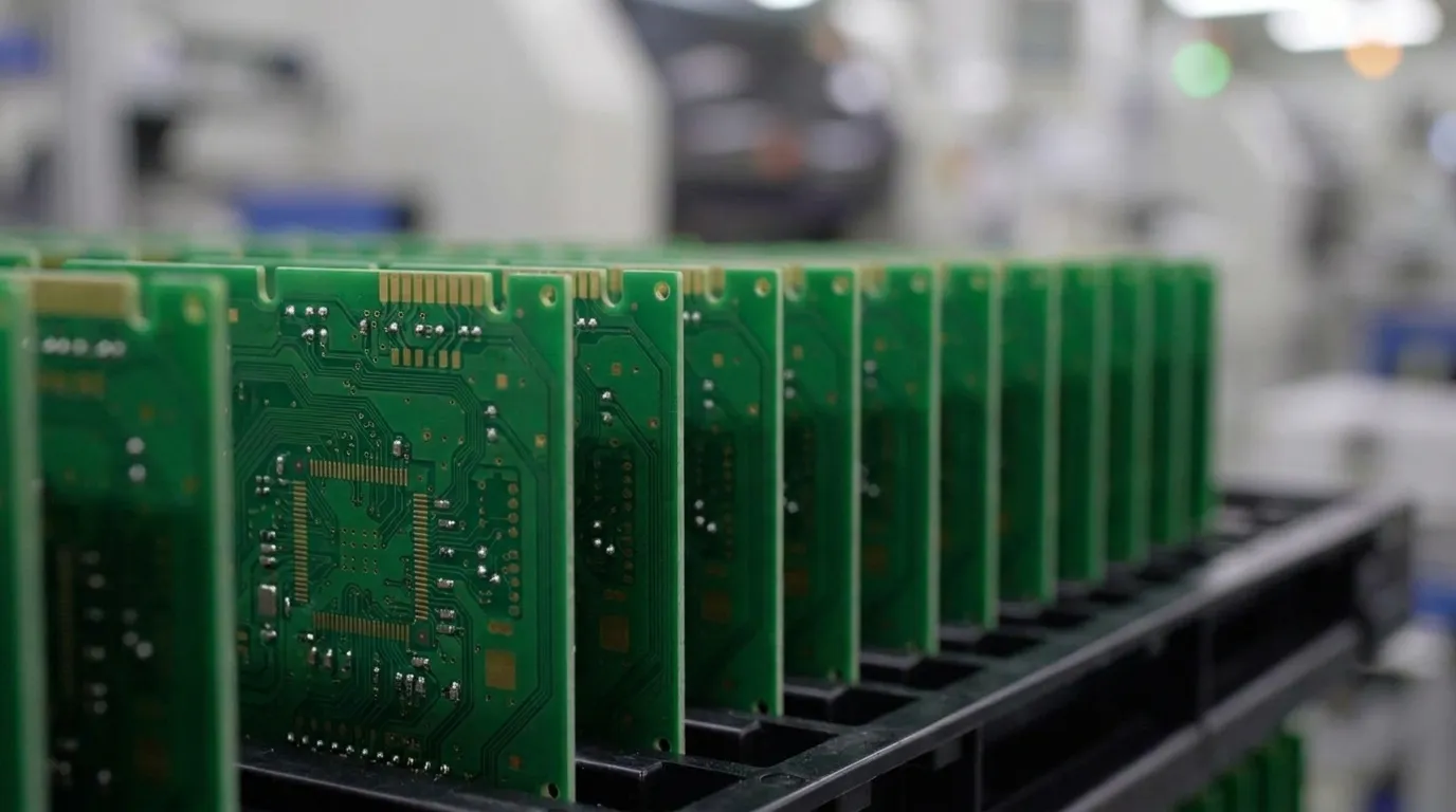
Key Takeaways for Flip Chip Packaging
-
Flip chip packaging mounts the die face-down using solder bumps or copper pillars, eliminating wire bonds and shortening electrical paths.
-
This structure supports higher I/O density and provides direct thermal access to the die surface for improved heat removal.
-
Underfill selection and process control are critical to long-term reliability in aerospace, defense, automotive and medical environments.
-
Underfill redistributes thermomechanical stress and extends fatigue life under repeated thermal cycling.
-
Pro-Active Engineering consolidates flip chip design, assembly, thermal management and ITAR-compliant manufacturing into a single U.S. workflow. Request a quote to evaluate the next high-reliability program.
Where Flip Chip Packaging Delivers the Most Value
Flip chip interconnects address distinct performance requirements across regulated and high-reliability sectors, with each industry prioritizing different combinations of thermal, electrical and mechanical performance. The following sections outline how flip chip packaging supports high-performance computing, automotive systems, aerospace and defense, RF modules and medical electronics.
Flip Chip Packaging Process Flow and Reliability Controls
The flip chip process begins with bump formation on the die, using copper pillar, solder or gold bump structures. Substrate preparation and flux application follow. The die is then placed face-down and reflowed to form electrical and mechanical bonds.
After reflow, the gap between the die and substrate is filled with an epoxy-based underfill material. Underfill selection directly determines long-term reliability. Underfill redistributes thermomechanical stress across the entire chip surface and is engineered with ceramic particles to match solder expansion, dramatically increasing fatigue life under repeated thermal cycling in harsh environments. Material selection must reflect the end-use environment, including temperature range, vibration profile and moisture exposure.
Integration with PCB assembly works best when flip chip attach functions as part of a unified manufacturing workflow, not a separate subcontract step. Traceability documentation, including lot records, process parameters and inspection data, should flow continuously from bump formation through final board-level test. In regulated programs, this documentation chain supports compliance audits and failure analysis throughout the product lifecycle.
Flip Chip vs Wire Bonding Design Tradeoffs
Wire bonding and flip chip each serve distinct design requirements. Wire bonding remains appropriate for lower I/O, cost-sensitive applications. Flip chip is the preferred interconnect for high-frequency, high-density and thermally demanding designs.
The electrical difference is significant. Wire bonding introduces inductance that limits performance above a few gigahertz, while flip-chip copper pillar bumps reduce interconnect inductance. This reduction explains why most high-performance processors, GPUs and FPGAs manufactured today use flip chip attach.
I/O density follows the same pattern. Flip chip packaging allows solder bumps across the entire bottom surface of the die rather than only around the edges. This approach enables far more I/O points on the same chip area than wire bonding. Wire-bonded packages such as QFP are constrained to perimeter connections, while flip chip scales with die area.
Thermal performance also favors flip chip. The face-down orientation in flip chip packaging creates a shorter thermal path from the chip to its heat sink, which draws heat away more efficiently than wire bonding. For high-power applications, this difference becomes a reliability factor rather than a simple performance preference.
The tradeoffs are real. Flip chip requires finer substrate tolerances, underfill processing and more rigorous DFM discipline, which increases design complexity and manufacturing cost. Wire bonding avoids many of these requirements, which makes it more forgiving at the design stage and less capital-intensive to rework. The decision therefore depends on whether gains in frequency, I/O count, thermal load or reliability justify the additional engineering investment.
Flip Chip Thermal Management Considerations
Thermal management is the primary reliability challenge in flip chip designs as power density increases in AI accelerators and high-reliability electronics. Thermal dissipation is the primary reliability challenge in densely stacked architectures, where heat fluxes can exceed levels manageable by conventional thermal interface materials, requiring thermal management to be integrated from the architecture phase.
The flip chip die orientation places the backside directly accessible for heatsink attachment or thermal interface material application. This structure shortens the thermal path compared with wire-bonded packages, where heat must travel through the substrate before reaching any external thermal structure.
In harsh environments, engineered solutions extend beyond standard heatsink attachment. Advanced thermal interface materials, direct thermal path PCB constructions, metal-core substrates and silver sintering each address specific thermal resistance challenges. Repeated thermal stress from CTE mismatch between silicon, substrates, solder and underfill can produce solder-joint fatigue, package warpage, interface delamination and interconnect degradation, which makes material selection and process control critical to long-term reliability. These thermal challenges are most acute in high-power computing applications, where power densities continue to rise.
High-Performance Computing and AI Accelerators
GPU and AI accelerator packaging represents the fastest-growing product segment in the flip chip technology market, driven by generative AI infrastructure build-out. High-performance computing and GPUs together account for a significant share of United States flip-chip demand, followed by networking and data center ASICs.
The 2.5D and 3D IC packaging market for AI accelerators continues to grow as designs shift from monolithic die scaling to heterogeneous integration. Flip chip interconnects are foundational to these architectures, enabling the fine-pitch bump arrays that connect logic tiles, memory stacks and interposers.
Engineering teams designing into HPC or AI accelerator programs benefit from DFM integration at the earliest layout stage. Bump pitch, substrate routing density, underfill compatibility and thermal path must all be resolved before prototype build, not after. Pro-Active Engineering embeds DFM into the design phase, which ensures that flip chip designs are production-ready before the first prototype is assembled. Discuss HPC or AI accelerator flip chip requirements with the engineering team.
Automotive Powertrain and ADAS Electronics
Automotive and transportation end-use in the flip chip technology market continues to grow, driven by ADAS, EV power and infotainment SoCs. Automotive-grade flip chip packaging for ADAS and power management ICs uses specialized underfill materials and extended reliability qualification cycles.
Automotive applications demand reliability across wide temperature ranges, vibration profiles and long service cycles. Flip chip shorter interconnect length and underfill-reinforced solder joints address these requirements more effectively than wire-bonded alternatives in high-density automotive SoC packages. Thermal management is equally critical in powertrain and ADAS applications, where sustained high-power operation must not degrade interconnect integrity over the vehicle service life.
Aerospace and Defense Ruggedization
Aerospace and defense represent a significant portion of flip chip technology market revenue, supported by trusted-foundry packaging demand. This segment commands the highest per-unit pricing due to ITAR/EAR compliance requirements and extended qualification timelines.
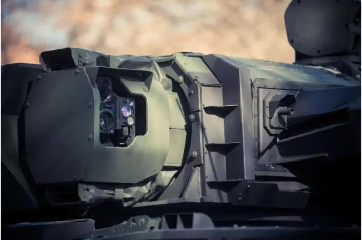
Domestic, ITAR-compliant manufacturing functions as a program requirement rather than a preference for most defense electronics. A substantial share of flip-chip packaging value consumed in the United States is supplied through imports from Taiwan, South Korea and Japan, which creates geopolitical supply-chain risk for defense, aerospace and critical infrastructure applications.
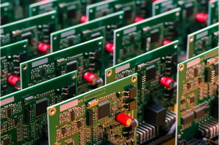
Pro-Active Engineering is ITAR-registered and maintains full traceability, controlled documentation and access procedures aligned with DDTC requirements. Aerospace and defense customers gain a single accountable U.S. partner for advanced interconnect design, flip chip assembly, ruggedization and system integration without routing sensitive program data or hardware through offshore supply chains.
RF and 5G Flip Chip Modules
Telecommunications end-use in the flip chip technology market continues to grow, driven by 5G and 6G base station and RF front-end module scaling. The RF and millimeter wave segment uses gold bump and specialized solder bump flip-chip interconnects that minimize parasitic inductance at high frequencies.
At millimeter-wave frequencies, interconnect parasitics become a primary design constraint. Flip chip short, direct bump connections reduce parasitic inductance and resistance compared with wire bonds, which preserves signal integrity at frequencies where wire bond length becomes a significant fraction of the signal wavelength. Glass interposers offer improved signal integrity, lower loss and better thermal performance than silicon, with pilot production underway and primary target applications in photonic integration and high-frequency RF.
Medical Electronics and Flip Chip Reliability
Healthcare industries apply flip-chip semiconductor technologies in medical imaging systems, diagnostic equipment and wearable health monitoring devices. Compact form factor, high I/O density and long-term reliability are the primary drivers for flip chip adoption in medical electronics.
Medical programs require full traceability, disciplined documentation and manufacturing processes that support regulatory submissions. Pro-Active Engineering ISO 9001:2015 certification, Nadcap accreditation and integrated quality management system provide the documentation infrastructure that medical device programs require from prototype through production.
How Pro-Active Engineering Supports Flip Chip Transition
Transitioning from wire-bonded or standard SMT designs to flip chip interconnects introduces process complexity at every stage, including design, substrate selection, underfill, assembly and test. Vendor fragmentation at any of these stages can create accountability gaps and late-stage manufacturability failures.
Pro-Active Engineering consolidates flip chip design, assembly, thermal management, ruggedization, testing and system integration into a single workflow, ensuring the DFM discipline described earlier carries through to production without translation loss between separate vendors.
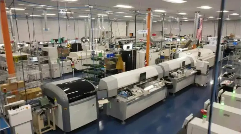
Production-ready prototypes are built using the same processes, equipment and quality controls as full production runs. This approach means that a flip chip assembly validated at the prototype stage scales directly into volume manufacturing without process requalification. Begin a flip chip prototype and production review with a single U.S. partner.
For defense and aerospace programs, the compliance infrastructure described earlier extends across the entire assembly lifecycle, from initial DFM review through final system integration. Program managers gain a domestic partner accountable for every phase of assembly and documentation.
Frequently Asked Questions
What industries benefit most from flip chip packaging?
Flip chip packaging delivers the greatest performance gains in applications where I/O density, signal bandwidth, thermal dissipation or compact form factor act as primary design constraints. High-performance computing, AI accelerators, automotive ADAS, aerospace and defense electronics, RF and millimeter-wave modules and medical imaging systems are the primary beneficiaries. In each of these sectors, the combination of shorter interconnect paths, area-distributed I/O and direct thermal access addresses limitations that wire-bonded packages cannot resolve at advanced node densities.
How does flip chip packaging affect total cost of ownership for mission-critical programs?
The per-unit cost of flip chip assembly is higher than wire bonding or standard SMT at equivalent volumes. Total cost of ownership across a program lifecycle also accounts for rework rates, field failure rates, redesign cycles and vendor management overhead. Flip chip superior reliability in thermally and mechanically demanding environments reduces field failures and extends service intervals.
Integrating DFM from the design phase, rather than discovering manufacturability issues at the prototype stage, eliminates costly late-stage redesigns. For regulated programs with long qualification cycles, a single accountable partner managing design through production reduces the administrative and risk costs of vendor fragmentation.
What compliance and traceability requirements apply to flip chip assembly in aerospace and defense programs?
Aerospace and defense flip chip programs typically require ITAR registration, AS9100 quality management, full lot traceability from raw materials through finished assembly, controlled documentation practices and workmanship standards aligned with IPC-A-610 Class 3. ITAR registration restricts access to controlled technical data and hardware to authorized personnel and facilities, which affects how design files, assembly records and test data are handled throughout the supply chain. Programs with Nadcap requirements add process-specific accreditation for soldering, inspection and coating operations. Pro-Active Engineering holds all of these certifications and accreditations, which provides a compliant domestic manufacturing environment for sensitive programs.
What is the difference between flip chip and wire bonding for high-frequency RF applications?
Wire bonding introduces parasitic inductance that degrades signal integrity at high frequencies. As operating frequency increases into the gigahertz and millimeter-wave range, bond wire length becomes a meaningful fraction of the signal wavelength, which creates impedance discontinuities and insertion loss. Flip chip interconnects are shorter and distribute connections across the die surface, which reduces parasitic inductance and resistance. For RF front-end modules, 5G base station components and millimeter-wave devices, flip chip is the preferred interconnect because it preserves signal integrity at frequencies where wire bonding performance degrades measurably.
Can flip chip assembly be integrated with standard PCB assembly in a single production workflow?
Flip chip assembly can integrate with standard PCB assembly when supported by deliberate process planning. Flip chip attach, including bump formation, placement, reflow and underfill, must be sequenced with standard SMT and through-hole operations in a way that protects both the flip chip assembly and adjacent components. Underfill cure cycles, reflow profiles and board handling procedures must remain compatible across the full assembly.
When flip chip and standard SMT operations are managed by separate vendors, process compatibility gaps frequently emerge at the integration stage. A single manufacturing partner that performs both flip chip assembly and PCB assembly within one workflow eliminates this risk and maintains continuous traceability across the full board build.
Conclusion: Flip Chip Evaluation Framework and Next Steps
Flip chip packaging is the appropriate interconnect choice when a design requires high I/O density, low parasitic inductance, direct thermal path access or compact form factor in a reliability-demanding environment. The decision to transition from wire bonding or standard SMT to flip chip should be evaluated against the following criteria.
-
The design requires I/O counts or signal frequencies that exceed wire-bonded package capabilities.
-
Thermal dissipation has become a reliability constraint that the current package architecture cannot address.
-
The program operates in aerospace, defense, medical or automotive sectors with compliance and traceability requirements.
-
Domestic, ITAR-compliant manufacturing is required for program security or regulatory reasons.
-
DFM is integrated from the layout stage rather than evaluated only after design completion.
-
The current supply chain lacks a single accountable partner from design through production, with multiple vendors managing separate phases.
Programs that meet multiple criteria above are strong candidates for flip chip transition and for consolidating design-to-production responsibility under a single U.S. partner. Pro-Active Engineering provides integrated flip chip design, assembly, thermal management, ruggedization and system integration with full traceability and ITAR-compliant domestic manufacturing. Begin the evaluation with the Pro-Active Engineering team.