
Key Takeaways for Defense PCB Potting
- PCB potting defense encapsulates circuit boards in cured polymer to block tampering, reverse engineering and environmental damage. It works best as one layer in a broader security strategy.
- Epoxy, silicone and polyurethane each present distinct tradeoffs in hardness, tamper evidence and reworkability. Material selection must align with the program threat model and service needs.
- Integrating potting with cryptographic controls, tamper meshes, inner-layer routing and secure elements during design creates a defense-in-depth architecture that is harder to defeat.
- Consolidating design, assembly, coating and potting with a single ITAR-registered domestic partner reduces compliance gaps, supply-chain exposure and traceability risks across the lifecycle.
- Pro-Active Engineering provides integrated PCB design, assembly, conformal coating, potting and system integration under one roof; discuss program requirements with the team.
The Problem: Potting Alone Does Not Secure Mission Hardware
Treating potting as a standalone security control creates program risk. Controlled reverse-engineering demonstrations have shown that epoxy potting alone does not prevent recovery of silkscreen markings, circuit layout or component locations when an adversary applies physical or thermal techniques. Potting raises the cost and difficulty of an attack. It does not eliminate the threat.
Vendor fragmentation compounds this problem. When design, prototyping, assembly, coating and potting are distributed across separate suppliers, communication gaps emerge. Manufacturability issues surface late. Traceability chains break. Compliance exposure grows at every handoff. An integrated workflow, where potting is planned during PCB layout rather than added after assembly, closes those gaps and reduces program risk.
Choosing Epoxy, Silicone or Polyurethane for Defense Potting
Three polymer families dominate defense potting applications: epoxy, polyurethane and silicone. Each presents a different profile of hardness, tamper evidence, reworkability and environmental resistance. Material selection depends on the program threat model, operating environment and serviceability requirements.
Epoxy compounds cure to high hardness, bond strongly to metals and ceramics and resist removal. Destructive methods such as milling, routing or chemical stripping typically damage the underlying assembly. That irreversibility makes epoxy the strongest choice for tamper evidence in permanent, non-field-serviceable assemblies. The tradeoff is brittleness under wide thermal cycling and poor reworkability.
Silicone compounds remain elastic across a wide operating temperature range and absorb vibration and thermal cycling stress. Programs often select silicone for field-serviceable military and aerospace connectors because it can be cut, peeled and removed with hand tools. That reworkability reduces tamper evidence compared with epoxy.
Polyurethane compounds occupy a middle position. They offer adjustable hardness, good vibration damping and moderate moisture resistance. Softer polyurethane formulations can be partially removed by heat softening. That behavior limits their tamper-evidence profile relative to hard-cure epoxy. Polyurethane is a practical choice when some reworkability is required and the operating temperature range is moderate.
The decision framework for defense programs should weigh these factors:
- Permanence vs. serviceability: field-replaceable assemblies favor silicone, while permanent security-critical assemblies favor hard-cure epoxy.
- Thermal environment: wide temperature swings with frequent cycling favor silicone flexibility, while stable high-heat environments favor epoxy thermal stability.
- Tamper-evidence priority: programs where physical attack resistance is paramount favor epoxy and its destructive-removal requirement.
- Regulatory and qualification requirements: MIL-STD-810 and related standards define environmental test conditions that the selected compound must survive.
Tamper-Resistance Functions of Opaque Potting Compounds
Once a material is selected, its contribution to tamper resistance becomes the next focus. Opaque, hard-cure potting compounds serve two tamper-resistance functions simultaneously. They conceal component identity, circuit topology and silkscreen markings from visual inspection. They also require destructive physical or chemical action to access the board, which leaves evidence of intrusion and risks destroying the assembly.
Opaque epoxy potting can deter reverse engineering for intellectual property protection on PCBs. Encapsulated circuits cannot be easily inspected, copied or modified, which raises the cost and skill threshold for any tampering attempt.
These properties create meaningful deterrents, not absolute barriers. A determined adversary with access to advanced laboratory techniques can still extract information from a potted assembly. That limitation defines why potting belongs in a layered security stack rather than standing alone.
Planning for Removal, Rework and Lifecycle Cost
Destructive de-potting is required for failure analysis of potted assemblies. That requirement creates longer repair cycles and higher field-service costs compared with conformal coating. Engineers must decide early in the design phase whether an assembly is intended to be permanent or field-serviceable. That decision drives material selection and affects lifecycle cost.
For permanent assemblies, hard-cure epoxy irreversibility becomes a feature. For assemblies that require periodic inspection, repair or component replacement, silicone hand-tool removability is the practical choice. Polyurethane occupies a middle ground for programs where some rework access is needed but full silicone flexibility is not required.
Process controls during potting are critical for reliability. Mix ratio management, temperature control and vacuum degassing help avoid soft spots, voids and insulation failures that compromise both environmental protection and tamper evidence. Defense program qualification requires that these controls remain documented and traceable.
Coordinating Potting with Cryptographic and Enclosure Controls
A complete physical security architecture for mission-critical electronics treats potting as one layer among several. Recommended complementary controls include removal of informative silkscreen markings, enabling read and write protections on microcontrollers and flash, firmware encryption and addition of resistive foil or tamper-evident layers.
Among these controls, tamper detection meshes deserve particular attention because they provide an active response capability that passive potting cannot. At the circuit level, these meshes consist of thin wires under components that trigger key erasure if the mesh is breached. They form a hardware layer that potting alone cannot replicate. When a tamper condition is detected, firmware must execute an irreversible response such as zeroizing cryptographic keys, invalidating device certificates and entering permanent lockdown.
A dedicated secure element or root-of-trust device stores keys immutably and verifies firmware signatures before execution. That cryptographic control operates independently of the physical potting layer. Routing sensitive traces on inner layers and shielding crypto modules with ground planes reduces probing and side-channel exposure before the assembly reaches the potting stage.
The integration sequence matters. Security features embedded in the PCB layout, inner-layer routing, tamper meshes and secure elements must be designed before the board is fabricated. Potting is applied after assembly. A partner that controls both design and ruggedization can coordinate these layers without the communication gaps that arise when separate vendors own each step.
Why a Single Domestic Partner Lowers Compliance and Supply-Chain Risk
ITAR controls technical data related to defense articles, including drawings, manufacturing instructions, test procedures and PCB layouts used to produce defense hardware. Every vendor handoff in a fragmented supply chain is a potential point of controlled data exposure, the communication and compliance gaps discussed earlier. Consolidating design, assembly and potting with a single ITAR-registered domestic partner reduces that exposure and simplifies compliance documentation.
Military electronics programs often require documentation for potting compounds to support qualification, including material certifications, process specifications, cure profiles and test results. When each manufacturing step involves a different vendor, that documentation must be collected, verified and reconciled across multiple quality systems with different formats and traceability practices. This fragmentation is operationally complex and creates audit risk.
Pro-Active Engineering holds ISO 9001:2015, AS9100, ITAR registration, JCP certification and Nadcap accreditation. Full traceability, from incoming material lots through assembly, coating and potting, is maintained within a single quality management system. Design for manufacturability is integrated from the first layout review, so potting requirements, thermal management needs and interconnect constraints are resolved before they become production problems.
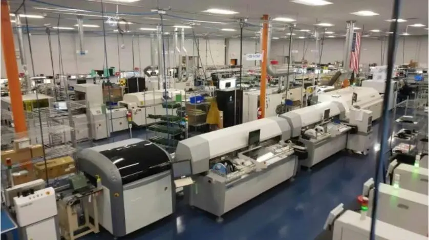
Defense and aerospace programs that engage Pro-Active Engineering gain access to wire bonding, flip chip assembly, advanced thermal management, conformal coating, potting, box build and system integration. All of these services operate under one roof, with one set of compliance records and one point of accountability.
Consolidate design and ruggedization workflows with a single ITAR-registered domestic partner.
Frequently Asked Questions
How does epoxy potting compare with silicone for tamper evidence in defense applications?
Epoxy and silicone serve different roles in defense potting programs. Epoxy cures to a hard, rigid state that cannot be removed without destructive methods such as milling, routing or aggressive chemical stripping that typically damage or destroy the underlying assembly. That irreversibility is the source of its tamper-evidence value. Any intrusion attempt leaves clear physical evidence and risks destroying the data or circuitry an adversary is trying to access.
Silicone, by contrast, remains elastic and can be cut or peeled away with hand tools. That behavior explains its use for field-serviceable connectors and assemblies that require periodic maintenance. For permanent, security-critical assemblies where tamper evidence is the priority, hard-cure epoxy is the stronger choice. For assemblies that must survive wide thermal cycling or require field repair access, silicone flexibility and reworkability outweigh its lower tamper-evidence profile. The right selection depends on the program threat model, serviceability requirements and operating environment, a decision best made during the design phase, not after assembly.
Can PCB potting alone prevent reverse engineering of mission-critical boards?
Potting acts as a meaningful deterrent that raises the cost, time and skill required to access circuit topology and component identity. Opaque, hard-cure compounds conceal silkscreen markings and component placement from visual inspection and require destructive action to breach. However, as noted earlier, laboratory techniques can still recover circuit information from potted assemblies despite these barriers.
Potting should be treated as one layer in a defense-in-depth architecture that also includes inner-layer routing of sensitive traces, tamper detection meshes that trigger key erasure on breach, secure elements that store cryptographic keys immutably, firmware encryption and enclosure-level protections. No single physical control is sufficient. The combination of hardware, firmware and physical barriers, designed together from the start, provides the most robust protection.
What documentation is required for ITAR-compliant potting in U.S. defense programs?
ITAR compliance for defense electronics manufacturing, including potting operations, requires registration with the Directorate of Defense Trade Controls and disciplined control of all technical data associated with the program. That data includes PCB layouts, manufacturing instructions, process specifications for potting compound application and cure, and test procedures.
Access to controlled data must be restricted to authorized U.S. persons, with documented access controls, personnel training records and audit logs. Supplier agreements must flow down ITAR handling requirements to any vendor involved in the manufacturing process. For the potting process itself, military qualification typically requires material traceability records, lot acceptance test data, process specifications and a qualification test matrix demonstrating that the potted assembly meets the specified environmental conditions.
Manufacturers must retain transaction records, technical data transfer records and related documentation for a minimum period defined by regulation. Engaging a single ITAR-registered partner that maintains all of this documentation within one quality management system reduces the compliance burden and audit risk compared with managing records across multiple vendors.
How should engineers combine potting with cryptographic hardware in layered security architectures?
The most effective approach integrates physical and cryptographic controls at the design stage rather than adding them sequentially. During PCB layout, sensitive traces should be routed on inner layers and shielded by ground planes to reduce probing exposure. Tamper detection meshes, fine conductive grids routed under critical components, should connect to a tamper detection circuit that triggers an irreversible response, such as zeroizing cryptographic keys and entering permanent lockdown, if the mesh is breached.
A dedicated secure element or root-of-trust device provides the cryptographic anchor, storing keys immutably and verifying firmware integrity before execution. Firmware encryption adds a software layer that remains effective even if an adversary physically accesses the board. Potting is then applied over this layered foundation, adding the physical barrier that conceals component identity and requires destructive action to breach.
The sequence matters. Cryptographic and tamper-detection features must be designed into the board before fabrication. Potting applied over a board that lacks these inner layers provides physical obscurity but not the autonomous response capability that a complete security architecture requires.
Conclusion: Evaluating PCB Potting Defense for Program Needs
PCB potting defense provides an effective physical barrier against tampering, reverse engineering and environmental stress. It does not form a complete security solution on its own. Material selection, epoxy for permanent tamper evidence, silicone for field serviceability and polyurethane for intermediate requirements, must align with the program threat model, operating environment and lifecycle requirements. Those decisions work best when made during PCB design, not after assembly is complete.
Integrating potting with inner-layer routing, tamper detection meshes, secure elements and firmware encryption produces a layered architecture that is harder to defeat than any single control. Executing that architecture through a single domestic partner that controls design, prototyping, assembly and ruggedization under recognized certifications eliminates vendor fragmentation, compliance gaps and traceability breaks that create program risk.
Pro-Active Engineering delivers that integrated capability. The integrated capabilities and certifications described above give defense and aerospace programs a single accountable partner throughout the manufacturing lifecycle.
Discuss potting and ruggedization requirements with Pro-Active Engineering’s team.