
Last updated: August 23, 2026
Key Takeaways for High-Power PCB Cooling
- Reducing power dissipation at the source through efficient components and precise conductor sizing forms the foundation of PCB thermal management.
- Heavy copper layers, thermal via arrays and metal-core substrates spread remaining heat laterally after source losses are reduced.
- Filled thermal vias, copper coins and embedded metal inserts create low-resistance vertical paths to the chassis or heatsink.
- Early thermal simulation, followed by infrared correlation, keeps junction temperatures within safe limits across the product lifecycle.
- Pro-Active Engineering delivers integrated simulation, fabrication, assembly and ruggedization under one roof, and teams can engage their thermal engineering team from day one.
Technique 1: Cut Component Power Loss to Limit I²R Heating at the Source
High-power PCB failures often start with Joule heating in conductors, where resistive loss scales with the square of current. Component selection, switching-frequency choices and efficiency-focused topologies reduce that loss at the source and lower the total heat the board must carry. Every watt removed at the source disappears from every downstream thermal path. Thermal vias and copper planes support this strategy but never replace careful power-loss reduction.
Integrating power-loss analysis into the DFM phase keeps thermal hardware decisions tied to real dissipation budgets instead of conservative assumptions.
Technique 2: Right-Size Power Conductors and Planes Before Adding Spreading Features
Wider conductors and thicker copper reduce I²R losses by lowering resistance, voltage drop and heat generation in the power path. Solid inner planes for power and ground, short distances between regulators and high-current loads and trace widths sized to current-carrying guidance all cut dissipation before any spreading technique is applied. A low-impedance PDN reduces electrical losses early and shrinks the thermal load that the rest of the board must handle.
Power distribution sizing during layout ensures thermal hardware is added only where loss reduction alone cannot meet temperature targets.
Technique 3: Use Heavy Copper Layers for Lateral Spreading in High-Current Regions
Copper conducts heat far better than FR-4, so heavy copper layers act as distributed lateral heat spreaders when paired with thermal via arrays under power devices. Hybrid stack-ups with heavy copper on outer layers for power and standard copper on inner layers for signals support high current while preserving fine-pitch routing. Manufacturability depends on relaxed trace-and-space rules that account for etch undercutting with thicker copper.
Pro-Active Engineering provides thermal and high-power PCB solutions that integrate heavy copper for mission-critical reliability.
Technique 4: Place Thermal Via Arrays Under Pads for Direct Vertical Heat Paths
Thermal vias reach their lowest vertical thermal resistance when placed directly under an exposed thermal pad instead of only around its perimeter. Arrays that tie into continuous copper planes without narrow necks spread heat laterally and reduce effective thermal resistance compared with isolated vias. Via count, geometry and fill type must align with fabricator process limits before layout release.
Advanced PCB fabrication capabilities at scale support optimized thermal via arrays from early prototypes through production builds.
Technique 5: Use Filled and Capped Via-in-Pad to Control Voiding and Improve Contact
Via-in-pad designs with filled and capped vias create flat soldering surfaces and stronger thermal performance than open vias. Epoxy-filled, copper-capped vias prevent solder siphoning during reflow on QFN thermal pads and meet IPC Class 3 requirements. Segmenting solder paste apertures on thermal pads further limits voiding while preserving reliable joint formation. This construction adds process steps and cost, so it must be planned at design entry instead of discovered at first article.
IPC Class 3 workmanship standards and automated X-ray inspection support consistent thermal-pad quality across prototype and production assemblies.
Technique 6: Add Copper Coins or Metal Inserts for Direct Paths Under Hot Packages
Copper coin vias use solid copper inserts embedded in the PCB core beneath heat sources to form a direct, low-resistance thermal path. Their conductivity exceeds that of plated vias or FR-4, so they move heat efficiently to lower layers or backside heatsinks while bypassing less effective via arrays. Precision milling, controlled lamination and surface planarization are essential, which makes fabricator capability a key selection factor.
Direct thermal path PCB technology and advanced interconnect methods extend to embedded metal constructions for demanding high-power designs.
Technique 7: Choose Metal-Core or Insulated Metal Substrates for Board-Level Spreading
Metal-core PCBs replace FR-4 with a metal base that spreads heat across the board and lowers thermal resistance more consistently than via arrays in standard laminates. Even basic aluminum PCBs improve thermal spreading compared with FR-4. Dielectric grade, base metal and thickness must match the application’s power density and dielectric-strength needs.

Engineered metal-core constructions support high-power defense, aerospace and industrial programs where FR-4 alone cannot meet thermal demands.
Technique 8: Use Silver Sintering for Low-Resistance Die Attach
Silver sintering replaces solder die attach with a porous silver layer that, once sintered, forms a thermal and electrical interface with lower resistance than solder alloys. The process avoids common reflow voiding mechanisms and produces joints that maintain integrity across wide temperature ranges. Tight process control during sintering protects joint quality and must be proven on production-representative hardware.
Pro-Active Engineering includes silver sintering in an integrated thermal workflow that spans design, assembly and test in a single facility.
Technique 9: Shape Copper Pours and Planes to Support Lateral Heat Flow
Solid planes for low impedance and close placement of regulators to high-current loads create short, efficient power paths that limit resistive loss. Copper pours tied directly to thermal pads without thermal-relief spokes reduce constriction resistance at pad boundaries. Plane splits, anti-pads and dense routing that break up copper coverage weaken lateral spreading and should be minimized in high-power zones. Accurate copper fraction modeling in simulation is essential because overestimated coverage often drives mismatch with measurements.
Thermal-aware copper pour strategies work best when built into the DFM workflow instead of added after routing.
Technique 10: Shorten Power Paths with Vertical Delivery and Embedded Passives
Vertical power delivery shortens the power path by moving regulation and passive components closer to the load, which reduces I²R losses that grow with current. Embedding passives in PCB cores or package substrates enables this architecture and frees board area. Design teams decide during architecture review how much loss can be avoided and how much efficiency gain is required, because this choice cannot be retrofitted after layout.
High-density interconnect and advanced packaging capabilities support vertical power delivery for high-reliability systems.
Technique 11: Tie PCB Thermal Mass into the Chassis with TIMs and Hardware
After loss reduction and spreading steps, remaining heat must leave the board through the chassis or a heatsink. Thermal interface material selection, contact pressure, surface flatness and attachment hardware all shape the resistance of this final path. Heatsinks should be sized for worst-case power dissipation so cooling remains reliable after efficiency gains. Heatsink design needs to start before PCB routing, because late changes often force costly re-spins.
Box build and system integration under one roof allow chassis-coupling decisions without the risk and delay of multi-vendor handoffs.
Technique 12: Protect Thermal Paths with Conformal Coating and Ruggedization
Conformal coating shields PCB assemblies from moisture, contamination and corrosion that damage solder joints and raise contact resistance over time. Degraded joints increase thermal resistance at the component-to-board interface and raise junction temperatures even when the original design met targets. Coating selection, coverage and cure must avoid masking thermal interfaces or adding insulating layers over heat paths. Ruggedization methods such as potting, underfill and mechanical reinforcement protect thermal joints under vibration and shock in defense and aerospace environments.
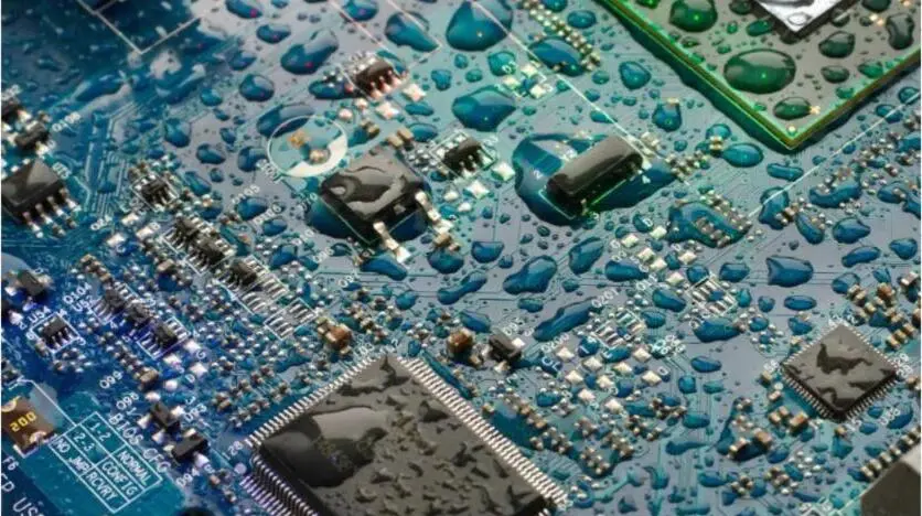
Pro-Active Engineering integrates conformal coating and ruggedization into the same workflow as PCB assembly so thermal performance remains stable from first build through field service.
Sequenced Approach to Reducing Heat in a PCB
An effective thermal strategy follows a three-level hierarchy. First, reduce dissipation at the source with efficient components, well-sized conductors and tight regulator placement near loads. Second, spread remaining heat laterally using copper planes, heavy copper layers, thermal via arrays and metal-core substrates. Third, couple the board’s thermal mass to the chassis with thermal interface materials, mechanical attachment and heatsink design. Applying spreading or coupling techniques before addressing source losses consumes board area and cost without solving the root cause. Thermal vias and copper planes work best as complements to proper PDN sizing.
PCB Thermal Simulation and Correlation Workflow
A practical PCB thermal simulation workflow starts by defining the decision, component limit, operating case and acceptance margin. Teams then freeze the BOM, stack-up, copper data, mechanical geometry, losses and environment before selecting model fidelity, assigning materials and contacts, applying loads and boundaries, meshing critical gradients, running convergence checks and comparing controlled variants.
Early thermal modeling during design helps surface issues before prototype measurement and correlation. Hardware correlation must match modeled locations, load, ambient temperature, orientation, enclosure, airflow and elapsed time. Thermocouples provide controlled point temperatures and infrared imaging captures spatial patterns. Common mismatch sources include overestimated copper coverage, missing thermal vias under high-power devices, incorrect power values and idealized convection boundaries. The loop closes when simulation and IR measurements align within the accepted margin and only uncertain parameters are adjusted.
Safe Temperature Limits for PCB Operation
Safe operating margins depend on component junction temperature limits, not only on board material ratings. Rising junction temperature accelerates device aging and shortens expected lifetime. Design teams build a thermal budget that keeps junction temperatures below rated limits under worst-case ambient and power conditions, with margin for manufacturing variation, aging and field uncertainty. Using worst-case maximum power ratings instead of realistic operating estimates often distorts temperature predictions. Defense, aerospace and medical programs typically apply more conservative margins than commercial designs to support long service cycles and strict reliability goals.
Understanding TG in PCB Materials
TG, or glass-transition temperature, marks the point where a PCB laminate shifts from a rigid, glassy state to a softer, rubbery state. Below TG, the laminate maintains mechanical and dimensional stability, which protects via integrity, layer registration and solder joint reliability. Above TG, Z-axis expansion increases, which stresses plated through-holes and weakens thermal contact across interfaces. High-TG laminates support applications where board temperatures approach or exceed standard FR-4 limits, including high-power industrial, aerospace and defense designs. Laminate choice must align with worst-case operating temperature and the fabricator’s qualified material list before design freeze.
Frequently Asked Questions
First Step in a PCB Thermal Management Strategy
The first step is reducing power dissipation at the source through component selection, conductor sizing and regulator placement. Spreading and chassis-coupling techniques follow only after source losses are minimized.
Best Time to Run Thermal Simulation
Thermal simulation should begin during architecture and layout, not after routing. Late simulation often uncovers issues that require board re-spins and schedule impact.
Metal-Core vs Heavy Copper PCBs for Thermal Control
A metal-core PCB replaces the FR-4 substrate with a metal base that spreads heat across the board surface. A heavy copper PCB uses thick copper layers to reduce I²R losses and spread heat laterally, often combined with thermal via arrays for vertical extraction.
Impact of Solder Voiding on Thermal Performance
Voids in thermal-pad solder joints reduce effective contact area between the component and the board and raise thermal resistance at that interface. Paste aperture design, via fill specification and reflow profile control help maintain the thermal path assumed in the design.
Value of an Integrated U.S. Manufacturing Partner
An integrated partner owns simulation, DFM, fabrication, assembly and test in one organization, so thermal decisions in design are validated on production-representative hardware without vendor handoffs. This structure reduces prototype-to-production disconnects that often cause late-stage thermal failures.
Conclusion: Sequenced Techniques and Integrated Execution
Advanced PCB thermal management works best in sequence: reduce dissipation first, spread heat second and couple to the chassis third. Each technique lowers a specific resistance in the thermal network, and the combined effect determines whether junction temperatures remain within safe margins over the product life. Simulation and infrared validation connect design intent to measured performance. A single accountable U.S. partner that owns engineering, fabrication, assembly, coating and system integration reduces the vendor fragmentation that turns thermal issues into program delays. Pro-Active Engineering delivers that integrated capability from concept through production, with full traceability and certifications for defense, aerospace, medical and industrial programs. Teams can begin a thermal management engagement with Pro-Active Engineering’s integrated design and manufacturing team.