
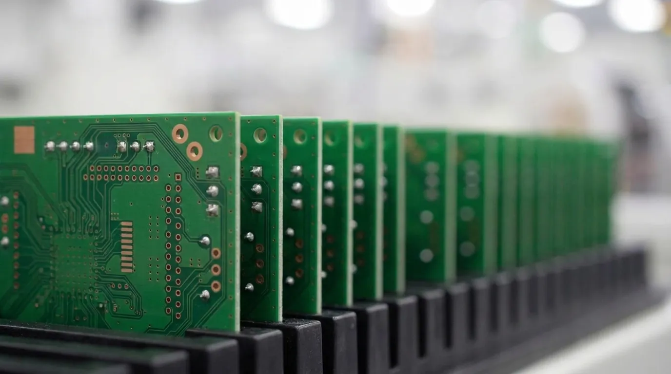
Key Thermal Lessons for HDI PCB Design
-
HDI PCB thermal management demands early planning because thin dielectrics and microvias concentrate heat near components and copper planes.
-
Via architecture sets the thermal foundation. Microvias support fine-pitch routing, while through-hole or hybrid schemes move concentrated heat more effectively.
-
Copper planes do most heat spreading. Generous planes under heat sources, tied together with thermal vias, reduce component temperature.
-
Material selection must match real power density. Standard FR-4 supports moderate loads with strong copper and via design, while higher-density designs need advanced substrates.
-
Pro-Active Engineering integrates thermal strategy into its DFM-first workflow, offering advanced solutions such as copper coins, silver sintering and direct thermal path technology.
Core HDI Thermal Management Workflow
Effective HDI thermal management follows a clear sequence of design decisions that build on each other.
-
Design the via architecture, choosing microvias, through-hole vias or a hybrid approach based on power density and routing limits.
-
Plan the stackup around copper planes as the primary heat-spreading elements.
-
Select materials that match actual power density requirements.
-
Place components to reduce thermal stress and maintain clear thermal paths.
-
Escalate to advanced techniques such as copper coins, silver sintering and direct thermal path technology when standard methods reach their limits.
-
Validate performance with thermal simulation and prototype testing before locking the design.
Thermal Via Design: Microvias and Through-Hole Vias
Via architecture is the first major thermal decision in HDI design and balances routing density with heat-carrying capacity.
Microvias enable the fine-pitch routing that defines HDI, but their small cross-sectional area limits thermal conductance. A filled microvia contains less copper than a standard plated through-hole via, so higher microvia counts are needed for similar vertical thermal conductance.
Through-hole vias provide a larger copper barrel for heat conduction and move significant heat to internal planes. They consume routing space and can affect signal integrity at high frequencies, so placement requires care.
The following guidance summarizes when to choose each via type based on routing and thermal needs:
-
Use microvias in signal-dense regions where small size supports fine-pitch components and tight routing.
-
Use through-hole vias or larger buried vias in thermal zones that do not require dense signal routing.
-
For high-power components, apply a hybrid approach with microvias for electrical connectivity and through-hole vias for thermal transfer.
Via sizing and placement decisions shape the effectiveness of the thermal path.
-
Use arrays of small vias instead of a single large via to move heat.
-
Place vias as close to heat sources as possible, ideally directly under thermal pads.
-
Use multiple vias in parallel for redundancy and scalable heat dissipation, and keep via sizes consistent across arrays for uniform plating.
Copper-filled microvias create a solid copper thermal path and support via-in-pad construction for fine-pitch BGAs. Copper-filled microvias deliver higher thermal conductivity than air-filled vias and can reduce junction temperature in power ICs with thermal via arrays. This approach improves thermal conductivity and mechanical strength but increases manufacturing complexity.
Reliability consideration. Staggered via configurations generally survive more thermal cycles than stacked configurations, which suits high-reliability aerospace and defense applications. Staggered vias reduce thermal fatigue failure under cyclic loading compared to stacked vias, and switching from stacked to staggered configurations has demonstrated yield improvements in production environments.
Stackup Design for Effective Thermal Spreading
The layer stackup forms the thermal backbone of an HDI board. Copper planes do most of the heat-spreading work, while vias act as bridges between layers.
Thermal simulation research illustrates this clearly. A hot pad with no plane underneath ran well above ambient temperature. Adding a small plane with one thermal via produced only modest improvement. Replacing the small plane with a large copper plane, even without thermal vias, reduced pad temperature dramatically. The plane performs most of the cooling.
Several stackup principles improve thermal performance:
-
Place a solid ground or power plane immediately below heat-generating components as the primary heat spreader.
-
Size this plane generously. A large copper plane provides more cooling than a small plane with thermal vias.
-
Use multiple ground and power planes as heat spreaders and connect them with thermal vias to build a vertical heat path.
-
Increase copper thickness on planes that serve as primary heat spreaders in high-current designs.
HDI buildup dielectrics are thin, which improves vertical thermal coupling between layers. A thinner core moves more heat between layers than a thicker core for the same temperature difference. The receiving copper plane then experiences more intense thermal loading and must be sized and connected accordingly.
Plane integrity matters. Dense BGA escape routing can fragment a power plane even when clearances pass design rules. Antipad patterns should be reviewed for power-plane neck-down and current crowding.
HDI boards face elevated warpage risk from asymmetric copper distribution and sequential lamination. Copper balancing prevents warpage by keeping copper distribution symmetric. Add copper thieving in sparse regions, keep copper percentage similar between corresponding layer pairs and avoid large copper pours on one side without matching copper on the other. Maintain copper percentage variation below a controlled threshold between corresponding layers.
Ground planes that serve as signal references also act as heat spreaders, which aligns electrical and thermal goals in HDI design.
Material Selection for HDI Thermal Performance
Material selection shapes both thermal behavior and manufacturability for HDI designs.
Standard FR-4 conducts heat poorly in the z-axis, so HDI thermal design should rely on copper spreading, thermal vias and local heat sinking rather than laminate conduction. FR-4 supports moderate power densities when paired with strong via arrays and copper planes, but performance limits appear as density rises.
High-Tg FR-4 improves structural integrity at elevated temperatures and reduces z-axis CTE, which improves delamination resistance in multilayer boards with dense vias. It often supports lead-free assembly and improves reliability under thermal cycling. However, it does not significantly improve thermal conductivity, and through-plane values remain comparable to standard FR-4.
Ceramic-filled laminates offer higher thermal conductivity than standard FR-4. They spread heat more effectively and reduce hot spots but increase cost and require different processing.
For extreme thermal demands, insulated metal substrate boards place a thermally conductive dielectric over an aluminum or copper base. The dielectric thermal resistance can be lower than an equivalent FR-4 layer for the same pad area. IMS boards are typically limited to single or double-sided constructions, so they do not support complex multilayer HDI routing alone.
Several guidelines help align materials with thermal needs:
-
Match material selection to measured or modeled power density requirements.
-
Consider the full material set, including dielectric thickness, reinforcement, resin behavior and copper profile.
-
Engage a manufacturing partner early because material choices affect manufacturability, lead times and reliability.
High-Tg materials with lower z-axis CTE reduce stress on plated through-holes and microvias during thermal cycling, which extends product life in mission-critical applications.
Component Placement and Layout for Heat Control
Component placement shapes thermal behavior and adds no material cost while reducing junction temperatures.
-
Spread heat sources. Avoid clustering high-power components in a single region. Spacing heat sources prevents overlapping thermal interference and localized hot spots.
-
Align with the thermal path. Place high-power components with a clear path to copper planes, thermal vias and the system cooling solution.
-
Use thermal pads and via arrays. Place via arrays directly beneath thermal pads to move heat into internal planes.
-
Account for airflow. In systems with forced or natural convection, orient components and board features to support the airflow pattern.
Signal microvias should not be assumed to replace a designed thermal path, and a dense field of small electrical microvias does not substitute for intentional heat-transfer structures.
Layout decisions that ignore manufacturing constraints often require redesign. Pro-Active Engineering integrates DFM into the design phase so layout decisions support both thermal performance and production yield before release. Request a quote for HDI PCB thermal management to engage Pro-Active’s engineering team early.
Advanced Thermal Management Techniques for HDI
Advanced techniques extend thermal capability when optimized vias, stackup planning, material selection and layout cannot meet requirements.
Copper coin technology. Copper coins, also called copper slugs or embedded coins, are thick copper blocks pressed into the PCB beneath high-power components. Embedded coins place thick copper directly under hot components and create a low-resistance thermal path from the component to the opposite board side or a heatsink. Copper coins suit components with concentrated heat flux, like high-power RF amplifiers and processors.

Silver sintering. Silver sintering is an advanced die-attach and thermal interface method that forms a bond with lower thermal resistance than traditional solder or thermal interface materials. Silver sintering benefits wide-bandgap semiconductors and other high-temperature, high-power applications where conventional materials degrade. It improves heat dissipation, extends product life and supports reliability in mission-critical designs.
Direct thermal path technology. A copper direct-thermal-path MCPCB places a controlled copper pedestal or coin directly beneath the component thermal pad. This structure bypasses the dielectric’s high thermal resistance in the primary vertical heat path while maintaining electrical isolation elsewhere. It suits high-power LED modules and other designs that need a controlled, low-resistance vertical path.
Heavy copper integration. Using heavier copper on heat-spreading planes increases cross-sectional area for lateral heat conduction, which reduces thermal resistance and improves current-carrying capacity.
These advanced techniques support high-power, mission-critical applications in aerospace, defense and medical devices where thermal performance margins must remain strong. They add cost and complexity, so teams apply them where standard approaches cannot meet requirements.
Pro-Active Engineering offers silver sintering, direct thermal path PCB technology, advanced metal-core constructions, heavy copper integration and integrated dielectric structures, all under one roof with engineering support from design through production.
Simulation and Testing for HDI Thermal Validation
Thermal simulation during design is essential for HDI PCBs because dense layouts make intuition unreliable.
Computational fluid dynamics software and PCB thermal analysis tools identify hot spots and confirm junction temperatures before design freeze. Addressing thermal issues during placement costs less than changes at signoff or after prototype builds.
IPC-2152 provides empirical, measurement-based guidance for conductor current-carrying capacity and accounts for board thickness, adjacent copper planes and dielectric thermal conductivity. IPC-2226 addresses HDI board design, including microvia structures and aspect ratio guidelines.
Prototype thermal testing then validates simulation and reveals manufacturing-related issues. Thermal imaging highlights hot spots that signal insufficient heat dissipation. A manufacturing partner that offers DFM analysis and thermal simulation helps reduce risk before production.
Partner With an Experienced HDI Manufacturer
Effective HDI PCB thermal management depends on early, engineering-driven decisions. Hybrid via design, stackup planning around copper planes, material selection matched to power density, component placement for clear thermal paths and targeted use of advanced techniques form a complete framework for high-density boards.
Discovering thermal issues only during prototype testing increases cost and delays programs. HDI thermal strategy must begin at the design stage.
Pro-Active Engineering provides integrated design and manufacturing, including thermal-optimized PCB architecture and advanced thermal management solutions. Pro-Active offers these advanced thermal solutions, including silver sintering and direct thermal path technology, under one roof. ISO 9001:2015, AS9100, ITAR registration, JCP certification and Nadcap accreditation support demanding aerospace, defense and medical applications.
Ready to solve HDI PCB thermal challenges? Request a quote from Pro-Active Engineering and partner with a team that designs, builds and tests high-reliability boards under one roof.
Frequently Asked Questions
What makes HDI PCB thermal management different from standard PCB thermal management?
HDI PCBs concentrate more power into less space using thinner dielectric layers, finer traces and microvia structures. These features that enable miniaturization also restrict heat flow. Standard thermal approaches based on large through-hole vias and thick copper pours do not transfer directly to HDI’s fine-feature environment. Thin dielectrics improve vertical thermal coupling between layers but concentrate heat at adjacent copper planes, which demands deliberate plane sizing and placement. Microvias contain less copper cross-sectional area than through-hole vias, so thermal via strategies must reflect that difference. HDI thermal management therefore requires a structured approach that treats via architecture, stackup design, material selection and component placement as a coordinated system.
When should a design move from standard FR-4 with thermal vias to advanced techniques?
The escalation decision depends on power density, component heat flux and reliability requirements. Standard FR-4 with an optimized via array and well-designed copper planes supports moderate power densities. As power density rises, the dielectric’s low thermal conductivity becomes a limiting factor that copper planes and via arrays alone cannot overcome. Copper coin technology suits components that generate concentrated heat flux and need a direct, low-resistance thermal path that bypasses the dielectric. Silver sintering fits wide-bandgap semiconductors and other high-temperature, high-power applications where conventional solder or thermal interface materials degrade over time. Direct thermal path technology supports designs where a controlled vertical heat path matters more than uniform board-wide conduction. For aerospace, defense and medical applications, teams often escalate earlier so reliability margins cover full service life.
How does stackup design affect thermal performance in HDI PCBs?
The stackup forms the thermal backbone of an HDI board. Copper planes act as the primary heat spreaders, and vias transfer heat between layers. Placing a solid ground or power plane directly below a heat-generating component is often the most impactful thermal decision in the stackup. The plane must be sized generously so it spreads heat sideways before passing it to deeper layers. HDI buildup dielectrics improve vertical thermal coupling, so the plane below a hot component experiences more intense thermal loading than in many conventional designs. Multiple ground and power planes connected by thermal vias create a vertical heat path through the board. Splits and cutouts in power planes weaken heat spreading and require careful review in critical regions. Copper balance between corresponding layers also matters because asymmetric copper distribution in HDI boards increases warpage risk and affects both thermal behavior and yield.
What role does thermal simulation play in HDI PCB design, and when should it be performed?
Thermal simulation is essential for HDI PCBs because dense, complex layouts make intuitive prediction unreliable. Simulation should begin during early floorplanning, before component placement is fixed, so hot spots can be addressed through layout changes instead of redesigns. Modern EDA tools support thermal analysis inside the PCB layout environment and flag junction-temperature issues at the placement stage. Simulation confirms that copper planes are sized correctly, that via arrays provide adequate thermal conductance and that material selection aligns with power density. Prototype thermal testing then validates simulation and highlights any manufacturing-related issues. The combination of simulation during design and thermal imaging during prototyping provides strong confidence that production hardware will meet thermal requirements.
How does Pro-Active Engineering support HDI PCB thermal management from design through production?
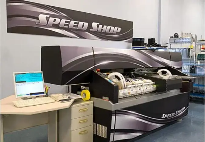
Pro-Active Engineering provides an integrated design-to-manufacturing workflow that builds thermal strategy into the design phase. The engineering team performs DFM analysis during design so thermal decisions such as via architecture, stackup planning, material selection and component placement remain manufacturable and reliable before the first build. For designs that need advanced thermal management, Pro-Active offers silver sintering, direct thermal path PCB technology, advanced metal-core constructions, heavy copper integration and integrated dielectric structures, supported by in-house engineering expertise. Rapid prototyping through the Speed Shop allows thermal designs to be validated quickly using the same processes as full production builds, which supports smooth scaling. Pro-Active certifications, including ISO 9001:2015, AS9100, ITAR registration, JCP certification and Nadcap accreditation, align with the documentation and traceability needs of aerospace, defense and medical programs.