
Last updated: August 6, 2026
Key Takeaways for PCBA DFM in Regulated Programs
- PCBA design for manufacturability services evaluate designs before production to prevent late-stage failures and reduce total cost of ownership.
- Early DFM integration is essential in regulated industries to avoid prototype-to-production disconnects, late ECOs and compliance gaps.
- A structured 8-step DFM checklist covering DRC, stackup, placement, solder mask, HDI, thermal analysis, BOM validation and final sign-off supports production readiness.
- DFA principles and thorough BOM validation reduce assembly defects and supply chain risk by addressing spacing, orientation, lifecycle status and sourcing early.
- Pro-Active Engineering delivers integrated PCBA design for manufacturability services under one roof, and teams can request a quote to start a technical review.
PCBA DFM Services for Regulated and High-Reliability Programs
Regulated industries face conditions that amplify the cost of late-stage failures. A design that passes simulation but fails assembly process validation can trigger engineering change orders, delay program milestones and create compliance documentation gaps that take weeks to resolve.
Several structural problems drive these outcomes:
- Prototype-to-production disconnect: When prototypes run on processes that differ from production, the transition exposes hidden manufacturability issues at the worst time.
- Late-stage ECOs: Design changes discovered during first article inspection or production qualification are costly and disruptive. They reset timelines and introduce new risk.
- Vendor fragmentation: Managing separate partners for design, prototyping, assembly, coating, testing and integration creates communication gaps. No single partner owns the outcome.
- Compliance gaps: Traceability, workmanship standards and documentation requirements in regulated industries demand disciplined process control across every handoff.
- Supply chain risk: Component obsolescence, counterfeit exposure and single-source dependencies create program vulnerability when sourcing is not validated early.
Integrating PCB DFM guidelines and DFA in PCB design from the start addresses these risks before they become program liabilities and sets up a repeatable framework for every new build.
8-Step PCBA DFM Checklist for Production Readiness
This eight-step checklist translates DFM principles into concrete actions. Each step targets a specific failure mode and should be completed before a PCBA design moves to production.
- Design Rule Check (DRC) in PCB: Run automated DRC to verify trace widths, clearances, via sizes and annular ring dimensions comply with fabrication and assembly process requirements. Resolve all violations before proceeding.
- PCB Stackup DFM: Confirm the layer stackup supports impedance control, signal integrity and mechanical stability. Validate that material selections and construction align with the assembly process and end-use environment.
- Component Placement Review: Evaluate component orientation, spacing and proximity to board edges. Confirm placement supports automated assembly, inspection access and rework access where required.
- Solder Mask Clearances: Verify solder mask openings, dam widths and paste aperture definitions match pad geometry and assembly process requirements to prevent bridging and insufficient solder joints.
- High-Density Interconnect DFM: For HDI designs, review microvia structures, via-in-pad configurations and sequential lamination requirements. Confirm the fabricator process capabilities align with the design intent.
- Thermal Analysis in DFM: Identify high-power components and thermal dissipation paths. Evaluate copper pours, thermal relief structures and any need for advanced thermal management solutions early in the design phase.
- BOM Validation for PCBA: Scrub the bill of materials for lifecycle status, lead time risk, single-source exposure and counterfeit vulnerability. Identify and qualify alternates before the design is released.
- Final DFM Review and Sign-Off: Conduct a cross-functional review with design and manufacturing engineering. Document findings, resolutions and any accepted deviations with supporting rationale.
DFA in PCB Design and Its Role in Preventing Assembly Defects
Design for assembly in PCB design focuses on layouts that support accurate, consistent and efficient automated and manual assembly. DFA addresses the physical realities of the assembly line, not only the electrical requirements of the schematic.
Key DFA considerations work together to reduce placement errors and inspection escapes:
- Component spacing: Adequate clearance between components prevents placement interference, allows inspection equipment access and supports rework without collateral damage.
- Orientation standardization: Consistent orientations for polarized components and ICs reduce placement errors and simplify visual inspection.
- Polarity marking: Clear polarity indicators on silkscreen and assembly drawings reduce the risk of reversed components reaching functional test.
- Pick-and-place accuracy: Well-placed fiducials, robust panel design and accurate centroid data allow automated placement equipment to perform reliably.
DFA failures rank among the most common sources of late-stage assembly defects. A component placed too close to a board edge, a missing fiducial or an ambiguous polarity mark can cause defects that surface during functional test or field operation. The DFA review described here directly prevents these placement errors and assembly defects that would otherwise appear during functional test or first article inspection.
BOM Validation for PCBA and Supply Chain Risk Reduction
BOM validation provides a structured review of every component on the bill of materials before production. For purchasing managers and program managers, this review offers a direct lever to reduce supply chain risk and protect program schedules.
A thorough BOM validation process follows a progression from risk identification to mitigation:
- Lifecycle status: Identify components approaching end of life or already discontinued. Qualify alternates before the design is frozen to avoid last-time-buy pressure or emergency redesigns.
- Alternative sourcing: Document approved alternates for single-source components. Validate that alternates are form, fit and function compatible and meet all applicable specifications.
- Counterfeit avoidance: Apply a structured counterfeit avoidance methodology to screen sourcing channels and procurement practices. Use authorized distribution channels and traceability documentation for components in regulated programs.
- Lead time risk: Flag components with extended lead times early so procurement can begin before they become schedule constraints.
Pro-Active Engineering integrates BOM scrubbing and lifecycle risk mitigation directly into the design and pre-production workflow rather than treating it as a separate procurement activity. Engineering teams and purchasing managers can request a quote to have Pro-Active review a BOM for supply chain risk before production.
Thermal and HDI DFM for High-Reliability Board Designs
Beyond component-level risks, high-reliability boards introduce design challenges that require specialized engineering analysis, particularly in thermal management and high-density interconnect structures.
High-reliability boards often combine thermal challenges with high-density interconnect requirements, with power-dense designs that must dissipate heat through tightly packed layer stackups. Thermal management and HDI design both require engineering analysis that goes beyond rule-checking because the interaction between heat dissipation paths and via structures directly affects long-term reliability.
Thermal analysis in DFM identifies heat dissipation requirements at the design stage, before layout decisions are locked. Key considerations include:
- Identifying high-power components and mapping thermal dissipation paths through the board and into the system
- Evaluating copper pour strategies, thermal vias and direct thermal path structures
- Determining whether advanced thermal management solutions such as silver sintering, metal-core constructions or integrated dielectric structures are required to meet reliability targets
For high-density interconnect designs, DFM review must address the specific process constraints of HDI fabrication. Tight-tolerance microvias, via-in-pad structures and sequential lamination sequences require close alignment between design intent and fabricator capability. Reviewing these elements during DFM, rather than at fabrication, prevents costly design iterations and schedule delays.
Pro-Active Engineering supports thermal management and advanced interconnect needs with silver sintering, direct thermal path technology, metal-core constructions, wire bonding, flip chip assembly and hybrid high-density assemblies. These capabilities operate within the same integrated workflow as design, prototyping and production.
How Pro-Active Engineering Delivers Integrated PCBA DFM Services
Pro-Active Engineering is a Wisconsin-based PCBA manufacturer that integrates design, rapid prototyping, assembly, conformal coating, testing and box build into a single accountable workflow. Founded in 1996, the company operates from a facility in Sun Prairie, Wisconsin, with a workforce of electronics professionals.
The integrated model embeds DFM from the first design review, not only at the handoff to manufacturing. Prototypes run on the same processes as production builds, so successful development assemblies scale without surprises. The Speed Shop delivers rapid prototype assemblies that support fast iteration cycles while maintaining process fidelity.
For purchasing and program managers, the single-partner model reduces vendor count, simplifies communication and provides full traceability under one quality management system. Pro-Active Engineering holds ISO 9001:2015 and AS9100 certifications, Nadcap accreditation and ITAR registration. The company is JCP certified (DD Form 2345) and aligns with NIST 800-171 and CMMC readiness requirements. All production is domestic, onshore and conducted under controlled, documented processes.
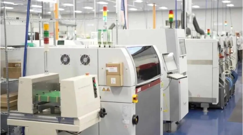
The integrated workflow covers a complete set of capabilities that directly address the DFM challenges described above:
- PCB layout and schematic design, including high-speed and high-density architectures
- Embedded control design, firmware and software development
- Rapid prototyping through the dedicated Speed Shop
- Surface mount and through-hole assembly with automated optical inspection
- Flying probe, in-circuit and functional testing
- Conformal coating, potting and ruggedization
- Advanced interconnect and packaging, including wire bonding and flip chip
- Thermal management solutions for high-power and high-current applications
- Box build and full system integration
- Documentation control and full traceability
Frequently Asked Questions
What is the difference between DFM and DFA in PCB design?
DFM, or design for manufacturability, covers design practices that make a PCB easier and more reliable to fabricate and assemble. DFA, or design for assembly, sits within DFM and focuses on layouts that support automated and manual assembly. DFA addresses component spacing, orientation, polarity marking and pick-and-place data accuracy. Both disciplines support production-ready designs and should be reviewed before release to manufacturing.
When in the design process should PCBA DFM services be engaged?
DFM services deliver the strongest impact during the schematic and layout phases, before the design is finalized. Early engagement allows the manufacturing engineering team to influence component selection, stackup construction, placement strategy and BOM sourcing decisions while changes remain low cost. Engagement after layout completion still adds value, but required changes carry greater cost and schedule impact.
How does BOM validation reduce total cost of ownership for regulated programs?
BOM validation identifies lifecycle risk, single-source exposure and counterfeit vulnerability before production. Addressing these issues early prevents last-time-buy emergencies, emergency redesigns and supply disruptions that can delay program milestones and drive unplanned costs. For regulated programs with long service cycles, proactive BOM management also reduces the risk of field failures caused by unqualified component substitutions.
What certifications should a PCBA manufacturer hold for defense and aerospace programs?
Defense and aerospace programs typically require manufacturers to hold AS9100 certification, ITAR registration and IPC-A-610 Class 3 workmanship compliance at a minimum. Nadcap accreditation applies to certain process categories. JCP certification, or DD Form 2345, is required for programs involving military-critical technical data. Full traceability, documented process controls and alignment with applicable soldering and rework standards are also expected. Pro-Active holds all of these credentials, as detailed in the section above.
Can a single integrated partner handle both low-volume prototypes and scalable production?
Pro-Active Engineering’s dedicated Speed Shop handles rapid prototype builds using the same processes as full production runs. This approach keeps new process variables out of the transition from prototype to production. The company supports orders as small as a single unit through high-mix, variable-volume production, with the same quality management system and traceability requirements applied at every volume level.
Next Steps to Initiate a PCBA DFM Technical Review
Programs that integrate PCBA design for manufacturability services early reach production with fewer ECOs, lower rework exposure and stronger compliance documentation. The first step involves mapping internal requirements such as design complexity, regulatory obligations, thermal and interconnect demands, BOM risk profile and production volume targets against a partner’s demonstrated capabilities.
Pro-Active Engineering’s engineering team conducts technical reviews that evaluate designs against fabrication and assembly process requirements, identify BOM risk and recommend thermal or interconnect solutions where needed. The review process surfaces issues while they remain inexpensive to resolve, supporting smoother launches and more predictable schedules.
Request a quote to initiate a technical review with Pro-Active Engineering and map a program’s DFM requirements from day one.