
Key Takeaways
-
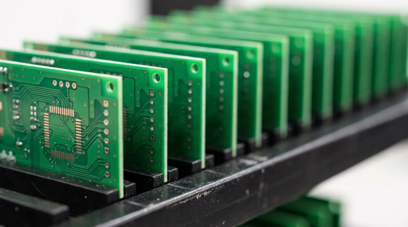
The die attach process uses controlled stages of die preparation, material application, placement, bonding or curing and inspection to set thermal path, mechanical stability and long-term reliability.
-
Material selection, from silver-filled epoxy and eutectic solder to silver sintering and die attach film, shapes thermal conductivity, electrical behavior, process complexity and reliability under thermal cycling and vibration.
-
Critical defects such as voids, die tilt, delamination, bleed-out and bond-line thickness variation require control and detection with X-ray, scanning acoustic microscopy and automated optical inspection to meet high-reliability standards.
-
Die attach quality influences downstream interconnect steps including wire bonding and flip-chip assembly, where issues such as die tilt or bleed-out can cause interconnect failures and reduced yield.
-
Pro-Active Engineering delivers integrated high-reliability die attach solutions with advanced interconnect capabilities and full traceability.
Five Core Die Attach Process Steps
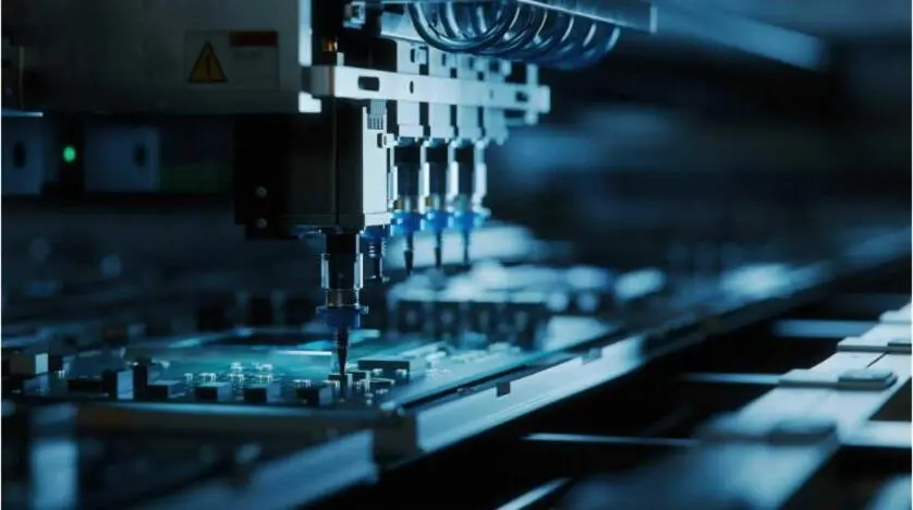
The standard die attach process follows five stages: die preparation, material application, die placement, bonding or curing and inspection. Each stage requires control to prevent defects that carry into downstream assembly and field service.
-
Die preparation and dicing: The wafer is diced into individual dies using a dicing saw, then cleaned and inspected for surface integrity.
-
Attach material application: Adhesive or bonding material is applied to the substrate by dispensing, stencil printing or film lamination using precision equipment.
-
Die placement: A pick-and-place system with a vacuum collet positions the die on the substrate with controlled placement force and accuracy.
-
Curing or bonding: The assembly passes through a reflow oven, sintering furnace or curing oven under a temperature profile matched to the attach material and, when required, a controlled atmosphere.
-
Inspection: The bonded assembly is inspected using X-ray, acoustic microscopy and automated optical inspection to verify bond quality before downstream processing.
Each step carries specific failure modes. Die preparation can introduce surface contamination if cleaning is incomplete. Material application can create voids or overflow when dispense volume or pattern control drifts. Die placement accuracy sets bond-line thickness uniformity and die position for downstream wire bonding or flip-chip attach.
The curing or bonding step must follow a temperature profile matched to the attach material. A fast ramp can trap volatiles and generate voids. Insufficient dwell time leaves the bond undercured. Bond-line thickness depends on several interacting factors: material volume, rheology, die and substrate flatness, tool parallelism and the thermal or curing profile.
Inspection closes the loop. A top-view optical camera detects missing or rotated dies but cannot confirm internal void level or full adhesive coverage. Internal bond quality requires X-ray or acoustic methods.
Engage Pro-Active Engineering on a die attach program that requires integrated control from material application through inspection.
Die Attach Material Families And Use Cases
Material selection sets thermal resistance, electrical conductivity, processing temperature and reliability under thermal cycling and vibration. The main die attach material families each align with specific thermal, electrical and reliability needs.
Conductive epoxy, especially silver-filled conductive epoxy, is the most common conductive die attach material in standard semiconductor applications. Silver-filled epoxy provides electrical and thermal conductivity through high silver loading in a polymer binder. It cures at relatively low temperatures, accommodates coefficient of thermal expansion mismatch through polymer flexibility and remains cost-effective for a wide range of assemblies. Its thermal conductivity is lower than solder or sintered silver, which limits use in high-power or high-junction-temperature designs.
Non-conductive epoxy supports applications where the die backside must remain electrically isolated from the substrate. Thermal conductivity is lower than conductive grades, which suits logic ICs, image sensors and stacked-die packages where all electrical connections route through top-side bond wires.
Eutectic solder forms a metallurgical bond at a defined alloy melting point and produces a low-thermal-resistance, low-void joint when parameters stay within tight limits. The eutectic die attach process is required by standards such as MIL-PRF-38534 and NASA-STD-8739.3 for Class B and Class S devices where epoxy is not allowed. Gold-tin eutectic is standard for high-power RF devices and hermetic packages. The inorganic bond does not outgas and resists thermal cycling better than organic adhesives. Eutectic die attach requires strict temperature profile control, a controlled atmosphere and precise alignment.
Solder paste with lead-free alloys such as SAC305 is the standard for commercial and industrial power modules. It provides strong thermal and electrical conductivity and runs on standard SMT reflow equipment. Voiding control often requires nitrogen atmosphere and, for demanding applications, vacuum reflow.
Silver sintering supports wide-bandgap power semiconductors such as SiC and GaN where junction temperatures exceed the service limit of silver-filled epoxy. Silver sintering paste fuses silver particles into a near-bulk-silver matrix with thermal conductivity higher than silver-filled epoxy and thermal cycling life that substantially exceeds solder. The process needs controlled pressure, controlled temperature, specialized tooling and silver or gold substrate metallization. Pro-Active Engineering includes silver sintering in production thermal management solutions for high-power and high-temperature applications.

Die attach film is a pre-formed adhesive film laminated to the wafer backside before dicing. Die attach film provides bond-line thickness controlled by film thickness, which removes dispensing variability that drives voids in paste processes. It serves as the standard interlayer dielectric in stacked-die packages such as 3D NAND and multi-chip modules. Conductive die attach film now supports applications that need both thermal performance and the process consistency of a film.
Epoxy suits standard assemblies where processing temperature, CTE accommodation and cost drive decisions. Eutectic or high-reliability solder supports hermetic, high-power or regulated applications that require inorganic bonds. Silver sintering supports wide-bandgap power devices and applications that demand long thermal cycling life. Die attach film supports stacked-die or high-density packages where bond-line uniformity is critical.
Discuss material requirements with the Pro-Active Engineering team to align die attach selection with thermal, electrical and reliability targets.
Die Attach Defects And Inspection Methods
Defect control in die attach matches the importance of the attach step itself. High-reliability programs pair each defect mechanism with an inspection method that detects it before the assembly moves downstream.
Voids are air gaps or gas pockets trapped in the bond layer. They form in three ways: dispense patterns trap air, volatile components outgas faster than they escape during cure or surface contamination prevents wetting. Voids reduce thermal conductivity, create stress concentration points under thermal cycling and can drive current crowding in power devices. Void distribution matters as much as total void area. A void under an active device region affects junction temperature more than a peripheral void of equal size. X-ray inspection is the production workhorse for void detection, with 2D multi-angle X-ray providing fast screening and 3D computed tomography providing volumetric analysis for root-cause work. Scanning acoustic microscopy complements X-ray by detecting interface-level separation that X-ray may miss.
Die tilt occurs when the die is not parallel to the substrate after placement and cure. Inconsistent adhesive viscosity, uneven dispense patterns and pick-and-place calibration drift commonly cause tilt. Die tilt shifts bond-pad height for downstream wire bonding and can move the sensing element reference plane in optical or motion-sensing devices. Automated optical inspection measures die tilt and fillet height in real time on the production line.
Delamination is separation at the die-to-adhesive or adhesive-to-substrate interface. It arises from CTE mismatch, surface contamination at bonding or adhesive modulus mismatch that concentrates shear stress under thermal cycling. Scanning acoustic microscopy is the primary non-destructive method for delamination detection. The acoustic impedance difference between a bonded interface and an air gap produces strong contrast even for thin separations that X-ray cannot resolve.
Bleed-out is excess adhesive that escapes past the die edge during placement. It can reach wire-bonding pads, sensor diaphragms or optical windows and block a clean metallurgical bond or obscure the signal path. Bleed-out arises from excess dispense volume, low adhesive viscosity or excessive placement force. AOI detects bleed-out at the die perimeter, and dispense-volume repeatability against a calibrated reference provides direct process control.
Bond-line thickness variation affects thermal resistance, mechanical stress distribution and the standoff height expected by the wire-bonding tool. Bond-line thickness that is too thick increases thermal resistance and CTE-driven stress. Thickness that is too thin risks direct die-to-substrate contact at surface high points. Bond-line thickness control relies on material volume, placement force, tool parallelism and thermal profile. In-line force monitoring provides a real-time proxy, and cross-sectional analysis confirms results.
In regulated programs defect documentation functions as a compliance requirement. IPC-A-610 Class 3 requires 100% visual inspection, strict documentation and near-zero deviation tolerance. X-ray inspection is required for hidden features where geometry prevents direct visual confirmation. Those defects matter most because die attach feeds directly into the next interconnect step.
Die Attach And Downstream Interconnect
Die attach and wire bonding form a sequential pair of complementary processes. Die attach secures the die mechanically and thermally to the substrate. Wire bonding then connects the die bond pads to package or board traces using fine gold, aluminum or copper wire.
After a die has been mechanically attached, it still requires electrical connection to the substrate structures through a separate bonding step. Wire bonding accounts for most die interconnect in standard packages. The two steps differ in purpose, equipment and failure modes, yet they remain tightly coupled in sequence.
The attach method shapes downstream interconnect performance. Die tilt introduced during attach changes the effective bond-pad height the wire-bonding tool must reach. Bleed-out on bond pads blocks clean metallurgical bonds. Bond-line thickness variation shifts the standoff geometry the bonding tool expects. A die attach process that passes initial inspection but delivers marginal bond-line control can still create wire-bonding failures that appear unrelated to attach.
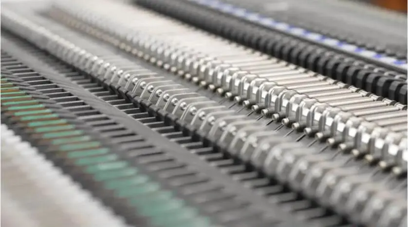
Attach material choice, bond-line thickness control and die tilt also influence flip-chip assembly. Flip-chip technology uses no long bond wires and provides compact chip-to-substrate connections. The chip is placed face-down with precise alignment, and solder bumps form the mechanical and electrical connection during reflow. Flip-chip attach places tight demands on substrate flatness, bump coplanarity and die planarity. Attach-layer voids and non-uniformity directly affect heat dissipation and mechanical strength in flip-chip packages.
Die Attach For High-Reliability And Regulated Programs
High-reliability die attach depends on process control, inspection rigor, documentation and traceability as much as on material choice. Regulated industries expect consistent performance across the entire build.
IPC J-STD-001 defines process and material requirements for soldered assemblies and emphasizes preventive control at every stage. IPC-A-610 Class 3 sets acceptance criteria for high-reliability assemblies and requires 100% inspection, full traceability and controlled rework. Class 3 assemblies must be planned from engineering review through production. A solder condition that passes under Class 2 can fail under Class 3, so the specified class must be confirmed before builds begin.
Pro-Active Engineering operates as a first-choice partner for high-reliability die attach and advanced interconnect. The integrated design-to-production workflow builds DFM into design so manufacturability, material selection and quality planning receive attention before production. Advanced interconnect and packaging capabilities include wire bonding, flip-chip assembly and hybrid high-density assemblies under one roof, which removes handoff risk between vendors. Thermal management solutions such as silver sintering, direct thermal path technology and metal-core constructions address thermal resistance targets for high-power and high-temperature applications.
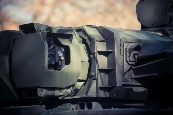
Pro-Active Engineering holds ISO 9001:2015 and AS9100 certifications, Nadcap accreditation, JCP certification, ITAR registration, NIST 800-171 alignment and CMMC readiness. The facility operates as an ITAR-registered manufacturing environment with access controls, data-handling procedures, documentation practices, foreign-national access restrictions per DDTC and personnel training records in place. Pro-Active Engineering builds high-reliability electronics for mission-critical defense and aerospace programs, certified to IPC-A-610 and IPC J-STD-001 with space addendum and traceability data capabilities.
The Speed Shop rapid prototyping capability delivers production-ready prototypes using the same processes as full-scale builds so process validation at prototype stage transfers directly to production. Single-partner scalability from prototype through volume production removes vendor fragmentation that can introduce compliance gaps and traceability breaks in regulated programs.
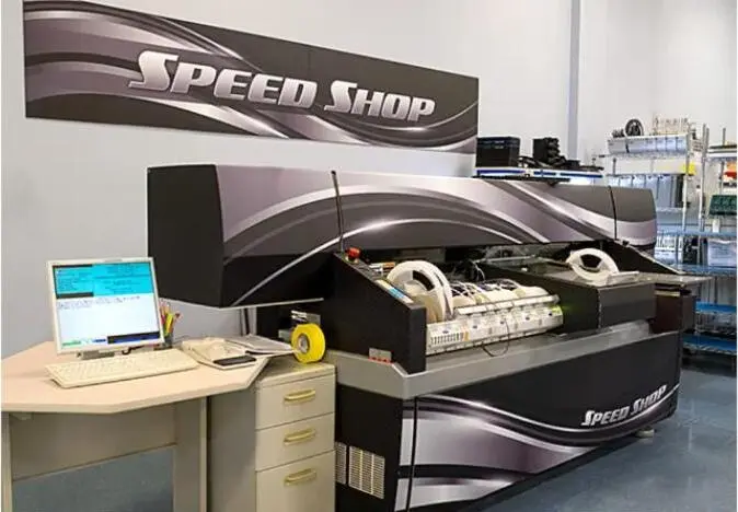
Share project details with Pro-Active Engineering to begin a design and manufacturing review.
Frequently Asked Questions
What Is the Difference Between Die Attach and Wire Bonding?
Die attach mechanically and thermally bonds a semiconductor die to a substrate, leadframe or package using an adhesive or metallurgical bond. Wire bonding then electrically connects the die bond pads to package or board traces using fine wire. Die attach must be completed and inspected before wire bonding begins, and attach quality, including bond-line thickness control, die planarity and pad cleanliness, directly affects wire-bonding yield and reliability.
How Does A Die Bonder Work?
A die bonder is the machine that executes the pick-and-place and material application steps of the die attach process. It presents and identifies the die from a diced wafer, picks the die using a vacuum collet without damage, prepares the bonding material and substrate, aligns and places the die under controlled force and height conditions and transfers the assembly downstream for curing or sintering. For epoxy die attach the die bonder places the die onto dispensed or printed adhesive and the bond is completed in a separate curing oven. For eutectic or solder die attach the bonder may apply heat during placement. For silver sintering the bonder handles placement and tacking while final densification occurs in a downstream sintering press. As noted earlier, bond-line thickness depends on material volume, rheology, flatness, tool parallelism and the thermal profile.
What Are the Steps in Die Preparation?
Die preparation begins with wafer dicing, in which a dicing saw cuts the wafer along scribe lines to singulate individual dies. After dicing, dies are cleaned to remove particles and surface contamination introduced during cutting. Cleaned dies are inspected for surface integrity because cracks, chips or metallization damage can cause latent failures that appear under thermal cycling or mechanical stress. For high-reliability applications, plasma cleaning is standard practice to remove organic contamination and activate the metal surface before attach. The prepared die is then presented to the die bonder for pickup and placement.
When Should Silver Sintering Or Die Attach Film Be Used Instead Of Epoxy?
Silver sintering suits wide-bandgap power semiconductors such as SiC or GaN where junction temperatures exceed the service limit of silver-filled epoxy or where reliability requirements include aggressive thermal cycling. Silver sintering produces a near-bulk-silver bond with thermal conductivity higher than silver-filled epoxy and thermal cycling life that substantially exceeds solder. It requires specialized equipment, controlled pressure and temperature and silver or gold substrate metallization.
Die attach film suits applications where bond-line thickness uniformity is critical and dispensing variability is unacceptable. This applies in stacked-die packages such as 3D NAND and multi-chip modules and in designs where bleed-out risk must be eliminated by design. Conductive die attach film now supports applications that require both thermal performance and the process consistency of a film.
Epoxy remains appropriate for standard assemblies where processing temperature, CTE accommodation and cost drive decisions and power density stays within the thermal conductivity range of silver-filled formulations.
How Are Voids and Die Tilt Detected?
Voids are detected primarily by X-ray inspection and scanning acoustic microscopy. Two-dimensional X-ray at multiple angles is the production workhorse for non-destructive void screening after reflow or cure and supports 100% inspection. Three-dimensional X-ray computed tomography provides volumetric analysis for root-cause investigation and golden-unit archiving. SAM detects interface-level separation and delamination because the acoustic impedance difference between a bonded interface and an air gap produces strong contrast even for thin separations. X-ray supports screening, and SAM supports sample validation and reliability lot inspection.
Die tilt is detected by automated optical inspection, which measures die planarity, fillet height and squeeze-out at the die perimeter in real time on the production line. Time-of-flight analysis in SAM can also reveal die tilt through package thickness variation and internal geometry mapping. In-line force monitoring during placement provides a real-time bond-line thickness proxy that offers more actionable data than post-cure cross-sectional sampling.
Conclusion And Next Steps
The die attach process functions as a reliability-critical manufacturing decision. Process parameters, material selection and defect control set long-term performance in aerospace, defense, medical and high-power applications. Effective outcomes require a partner with integrated design-to-production control, advanced interconnect capabilities and inspection and traceability infrastructure that support regulated programs.
Pro-Active Engineering brings wire bonding, flip-chip assembly, hybrid high-density assemblies, silver sintering and direct thermal path technology together under one roof, with ISO 9001:2015, AS9100, Nadcap, ITAR and JCP certifications supporting IPC-A-610 Class 3 and J-STD-001 workmanship requirements. The Speed Shop delivers production-ready prototypes that scale directly to volume manufacturing without process transfer risk.
Connect with Pro-Active Engineering to share project details and begin a design and manufacturing review.