
Last updated: August 17, 2026
Key Takeaways for Production-Ready Placement
- Assembly-process selection (wave or reflow) must be finalized first because it dictates every subsequent placement rule.
- Global and local fiducials, placed early with proper solder-mask clearance, support machine-vision accuracy and reduce placement defects.
- Mechanical constraints, thermal zones and rework-tool access should be resolved before electrical routing to avoid redesigns.
- Component orientation, spacing and test-point access must align with the chosen IPC-A-610 Class 2 or Class 3 workmanship standard.
- Pro-Active Engineering embeds these DFM rules from day one. Request a quote to start a collaborative review that prevents prototype-to-production disconnects.
Assembly-Process Decision Tree: Wave and Reflow First
Assembly-process selection is the first placement decision because it governs every constraint that follows. The choice between wave soldering, reflow soldering or a mixed-technology process determines component orientation rules, keep-out zones and thermal sequencing.

The decision follows this logic:
- Designs that include through-hole components that cannot convert to SMT require wave or selective soldering for those components.
- Designs with all surface-mount components use reflow as the primary process.
- Designs that mix SMT and through-hole on the same side use a mixed-technology process, and SMT components must be placed to survive the thermal exposure of the secondary process.
- Boards that require double-sided SMT run bottom-side assembly first, followed by top-side reflow, and bottom-side component mass must be evaluated for reflow retention.
A production DFM workflow begins with involving the EMS partner before finalizing Gerbers, so process selection becomes a design input rather than a late constraint.
Fiducial Placement for Machine Vision Accuracy
Once the assembly process is defined, the next step is establishing the reference system that automated equipment uses to execute that process. Fiducials provide that reference for paste printing, pick-and-place and AOI, and errors in fiducial placement propagate through the entire assembly sequence.
Global fiducials use a larger pad diameter with proportionally larger solder mask clearance and are placed as three noncollinear marks near board or panel corners to correct for X-Y offset, rotation and scaling across the entire board. This board-level correction handles gross positioning errors, but fine-pitch components require additional precision. Local fiducials use a smaller pad diameter and are placed as two marks diagonally outside critical components such as BGAs, QFNs and fine-pitch connectors to refine placement accuracy within the pick-and-place camera field of view.
A clear area around every fiducial must remain free of copper traces, silkscreen, text and solder mask encroachment, following IPC-2221 spacing guidance to maintain optical contrast. Silkscreen-only fiducials are unreliable, so copper pads are required for consistent machine-vision detection. For double-sided SMT assembly, each side must carry its own fiducial set.
In aerospace, defense and medical programs built to IPC-A-610 Class 3 standards, well-placed fiducials support consistent solder paste deposition, reduced component skew, improved BGA alignment and fewer latent defects.
Mechanical Constraints Before Electrical Placement
Mechanical constraints define the buildable envelope, so they must be resolved before component placement. Placing components before resolving mechanical keepouts forces layout revisions and can invalidate entire routing layers.
Component bodies must maintain clearance from the PCB edge to prevent mechanical stress damage during panel depaneling. When components must sit near the edge, orientation becomes critical, and the long axis should align parallel to the depaneling cut direction for even stress distribution on pads.
Board outlines, keepouts and component height limits derive from mechanical packaging and control routing density, layer usage and manufacturability on the electrical side. Effective ECAD-MCAD coordination keeps outlines, stiffeners and mounting holes aligned with layout so the design stays within buildable boundaries as the enclosure evolves.
Rework-tool access functions as a mechanical constraint. Successful PCB rework requires board support, preheat, localized heat, nozzle selection, airflow, contact method, extraction, shielding, temperature monitoring and cooling so tools can reach the target without collateral damage. Components placed too close to connectors, tooling holes or mechanical features restrict rework nozzle access and increase repair risk.
Thermal Balance and Decoupling Proximity
Mechanical constraints define where components can physically exist on the board. Thermal constraints define where they can operate without creating heat-related failures, so thermal planning must occur before routing begins. Thermal placement decisions made after electrical routing are reactive, while thermal decisions made before electrical routing are preventive.

Component placement in high-performance PCB design must account for heat flux, not electrical function alone. Two devices that dissipate identical power can create different thermal challenges depending on heat dissipation area and coupling to the PCB. Mutual heating between closely placed components such as converters and drivers produces nonlinear temperature rise that does not follow individual power ratings.
Tall and short components should be spaced to reduce shadowing and uneven heating caused by thermal mass variations. Decoupling capacitors must sit as close as practical to the power pins they serve, with short routing to minimize inductance. Many aerospace and telecom projects incorporate thermal simulation before prototyping to guide component placement and airflow decisions.
Wave-Direction Shadowing and Component Orientation
Wave soldering introduces a directional process variable that reflow does not. Components placed without regard to wave direction create solder shadows, where the wave cannot reach downstream pads because an upstream component blocks solder flow.
To reduce shadowing defects, taller components must be placed downstream of shorter components relative to the wave travel direction. Components with the same height should be staggered rather than aligned in rows perpendicular to wave travel.
For reflow assemblies, chip components should be oriented parallel to the conveyor direction in forced convection reflow ovens to balance heating across terminations and minimize airflow gradients. Engineers benefit from orienting all passive components consistently to simplify tape-and-reel feeding and reduce programming time for pick-and-place machines.
Pick-and-place optimization guidance recommends reducing head travel, grouping similar packages, minimizing nozzle changes and balancing feeder locations. These actions improve throughput and placement stability and address vibration and offset defects observed in production.
Test Access and AOI Placement Rules
Test access often becomes the most frequently skipped DFM category. Fab DRC tools automatically catch footprint and tolerance errors, but nothing automatically flags missing test points, which makes test access the most expensive category to retrofit after the first panel.
The test strategy, whether in-circuit, flying-probe, functional or boundary-scan, must be decided before layout begins. Required test points and access then can be reserved so probes and fixtures remain feasible after component placement, and test pads with traceable nets can be designed into the board before release.
AOI systems depend on unobstructed sightlines to component bodies and solder joints. AOI equipment specifies PCB surface and edge clearance zones as required keep-out areas for reliable automated optical inspection access. Components placed inside these zones reduce inspection coverage and increase false-call rates. AOI systems also rely on fiducials to define inspection regions and reduce false calls in high-density IPC Class 2 and Class 3 assemblies.
Qualitative Spacing for Class 2 and Class 3
IPC-A-610 defines two workmanship tiers relevant to most defense, aerospace and medical programs. The list below describes the qualitative difference in spacing expectations between Class 2 and Class 3 assemblies, without numeric values, because spacing requirements vary by component type, process and program-specific acceptance criteria.
- Component-to-component spacing: Class 2 provides clearance for automated assembly and inspection. Class 3 requires greater clearance to support rework, inspection and long service life, which often increases board area or layer count.
- Board edge clearance: Class 2 provides clearance to prevent mechanical damage during depaneling. Class 3 uses more conservative clearance to protect solder joints and component bodies under stress, so keepout zones must be defined before component placement begins.
- Rework-tool access: Class 2 prefers access but does not always mandate it by workmanship standard. Class 3 requires access to support repair without collateral damage per IPC-7711/7722, and nozzle clearance and thermal shielding must be verified during DFM review.
- Test-point accessibility: Class 2 recommends test points for functional verification. Class 3 requires test points on critical nets with single-sided probing preferred, so the test strategy must be defined before layout lock-in.
12-Step PCB Component Placement Sequence
This sequence integrates mechanical, thermal and test constraints before electrical placement and closes with EMS DFM sign-off to prevent prototype-to-production disconnects.
- Select the assembly process. Determine whether the board requires reflow, wave, selective soldering or a mixed-technology process.
- Import mechanical constraints. Load board outline, keepouts, mounting holes, connector locations and height restrictions from the mechanical model before placing any component.
- Place fiducials. Position global fiducials at board or panel corners and local fiducials adjacent to fine-pitch and BGA devices, and verify solder mask clearance and optical contrast.
- Place fixed mechanical components. Position connectors, mounting hardware, heat sinks and shields first, because these define the remaining placement envelope.
- Establish thermal zones. Identify high-power devices and assign them to thermal zones with copper spreading, airflow paths or thermal interface access, and separate heat sources from heat-sensitive components.
- Place power management and decoupling components. Position regulators, converters and decoupling capacitors close to the power pins they serve, within the thermal zones defined in step 5.
- Orient components for the selected soldering process. For wave assemblies, orient components to reduce shadowing relative to wave direction. For reflow assemblies, orient passives parallel to conveyor direction to balance heating.
- Place high-speed and RF components. Position these devices with short return paths and minimal via transitions, within the mechanical and thermal envelope already established.
- Place remaining active and passive components. Fill remaining board area while maintaining process-appropriate spacing between component bodies and from board edges.
- Reserve and verify test access. Confirm that test pads, programming headers and debug connectors are reachable by the selected test strategy, and verify AOI sightlines and keep-out compliance.
- Verify rework-tool access. Check that nozzle clearance exists around every component likely to require rework, and flag any component surrounded by taller neighbors or placed inside mechanical keepouts.
- EMS DFM sign-off. Submit the layout to the EMS partner for a formal DFM review against the selected assembly process, IPC-A-610 class requirements and production tooling constraints before releasing Gerbers.
Production-Ready Prototype Checklist
A prototype built with different processes than production will not predict production yield. This checklist confirms that the prototype and production builds share the same process baseline.
- Assembly process selected and documented before layout began
- Global and local fiducials placed with correct pad size and solder mask clearance on every assembly side
- Mechanical keepouts imported from MCAD and verified against component placement
- Board edge clearances meet the applicable IPC-A-610 class requirement
- Thermal zones defined and high-power devices placed within them
- Decoupling capacitors placed adjacent to power pins with short routing
- Component orientation verified for wave direction or reflow conveyor direction
- Component-to-component spacing meets the applicable IPC-A-610 class requirement
- Test strategy defined, and test pads, programming headers and debug connectors reserved and accessible
- AOI keep-out zones clear of component bodies
- Rework-tool nozzle clearance verified for all components
- BOM scrubbed for lifecycle risk and counterfeit avoidance per SAE AS5553B
- EMS DFM sign-off completed before Gerber release
How Pro-Active Engineering Applies This Workflow
Pro-Active Engineering is a Wisconsin-based PCBA manufacturer with ITAR registration, Nadcap accreditation, AS9100 certification and ISO 9001:2015 certification. The company operates an integrated workflow that connects PCB design, rapid prototyping, scalable assembly, conformal coating and system integration under one roof.
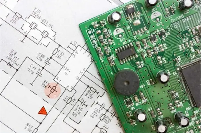
Key DFM principles are embedded in the design phase at Pro-Active Engineering. Engineering and manufacturing operate within the same workflow, so DFM constraints from the production floor become design inputs before layout begins, and staged DFM checks are applied before full-scale release.
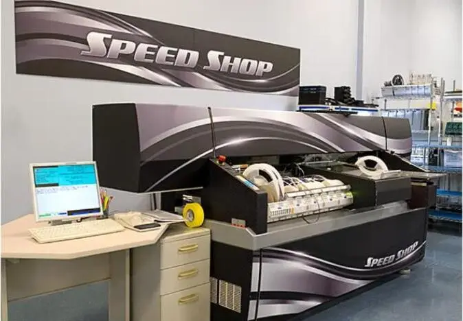
Prototypes are built through Pro-Active’s dedicated Speed Shop using the same SMT lines, inspection equipment and quality processes as production builds. This continuity means the production transfer is a process confirmation, not a process discovery.
Pro-Active serves defense, aerospace, medical and industrial programs that require IPC-A-610 Class 3 workmanship, full traceability and secure domestic manufacturing. Advanced interconnect capabilities including wire bonding, flip chip assembly and hybrid high-density assemblies extend the placement workflow into mission-critical packaging requirements that many standard EMS providers do not support.

Conclusion and Next Step
PCB component placement optimization for manufacturability functions as a sequenced discipline, not a checklist applied after routing. Assembly-process selection, fiducial placement, mechanical constraints, thermal zoning, wave-direction orientation and test access must all be resolved before electrical placement begins. When these steps are embedded in a DFM workflow validated by an integrated EMS partner, defect rates fall and production transitions become predictable.
Pro-Active Engineering applies this sequence from the first design review through scalable production, backed by ITAR registration, Nadcap accreditation and certifications that regulated programs require. One accountable onshore partner eliminates the vendor fragmentation that creates yield surprises and compliance gaps.
Frequently Asked Questions
Most Common Cause of Prototype-to-Production Disconnects
The most common cause is that prototypes are built using processes, equipment or workmanship standards that differ from the production line. When a prototype is hand-soldered or assembled on a general-purpose line without production-equivalent stencils, reflow profiles and inspection, prototype yield does not predict production yield. Defects that appear at production volume, such as tombstoning, solder bridging and BGA voiding, existed in the prototype process but did not appear because the sample size was small. Building prototypes on the same equipment and processes as production, with a formal DFM sign-off before Gerber release, provides the most reliable way to close this gap.
Best Timing for DFM Review in PCB Design
DFM review should begin before layout starts, not after Gerbers are complete. The most expensive DFM findings are those discovered after routing is locked, such as missing test points, components inside mechanical keepouts or orientation errors that require a board spin. Involving the EMS partner at the schematic and early layout stage allows assembly-process selection, fiducial requirements, thermal zone definitions and test strategy to become design inputs. A formal DFM sign-off before Gerber release confirms that the layout is buildable on the production line without modification.
How IPC-A-610 Class 3 Changes Placement Decisions
IPC-A-610 Class 3 applies to high-reliability assemblies where continued performance is critical and the end-use environment demands long service life. Class 3 workmanship expectations require more conservative component-to-component spacing, greater board edge clearance, verified rework-tool access and test points on critical nets. These requirements translate directly into placement decisions, so Class 3 layouts typically require more board area, higher layer counts or both to meet spacing and access requirements. Class 2 applies to general electronic products where some cosmetic imperfection is acceptable but full functionality is required. Identifying the applicable class before layout begins prevents the need to re-space components after the design is otherwise complete.
Role of Fiducials in Reducing Defects in High-Density Assembly
Fiducials act as reference marks that allow pick-and-place machines, solder paste printers and AOI systems to correct for board-to-board variation in position, rotation and scale. Without accurate fiducials, placement offsets accumulate across the board and increase the probability of component skew, solder bridging and BGA misalignment. In high-density assemblies with fine-pitch devices, even small placement errors can cause defects that remain hidden until functional test. Local fiducials placed adjacent to BGAs, QFNs and fine-pitch connectors provide a second correction layer within the camera field of view and improve placement accuracy for the most defect-sensitive components on the board.
Support for Prototypes and Production in One Program
Pro-Active Engineering manages programs from single-unit prototypes through scalable production within the same integrated workflow. The Speed Shop delivers rapid prototype assemblies using full production processes, so the transition to volume manufacturing becomes a process confirmation rather than a process change. Engineering, quality and manufacturing operate under one roof, which means the DFM constraints, workmanship standards and documentation practices established during prototyping carry forward into production without a handoff to a separate facility or team. This continuity supports defense, aerospace and medical programs where traceability and process consistency are compliance requirements.