
Last updated: August 15, 2026
Key Takeaways
- Bed-of-nails ICT delivers fast, repeatable structural verification when test access and fixture mechanics are planned early in the design phase.
- Fixture design, probe density, board support and pneumatic actuation are critical to avoiding mechanical stress and ensuring reliable contact on high-density PCBAs.
- Strict test-point placement rules, including pad size, spacing, clearance and BGA breakout access, directly determine achievable coverage and first-pass yield.
- Hybrid strategies that combine ICT with boundary scan, flying probe, X-ray and functional test close coverage gaps on boards with inaccessible BGA nets and complex digital interconnects.
- Pro-Active Engineering integrates ICT planning into the design phase of complex PCBA programs, and connects customers with the engineering team to align test strategy with production goals.
How Bed-of-Nails In-Circuit Testing Works
Bed-of-nails ICT is a structural test method in which a custom fixture presses an array of spring-loaded pogo pins against dedicated test points on a populated PCB. Each pin contacts a specific net, and the tester injects signals and measures component values, shorts, opens and polarity across the board netlist in a single fixture closure. The result is fast, repeatable electrical verification of board construction before functional test.
Fixture Design That Protects the Board
A bed-of-nails fixture uses a base plate, a probe plate drilled to match the board test-point layout and alignment features that register the board to the probe field. Pogo pins press into the probe plate and connect to the test system measurement channels.
Pin density, probe pitch and spring force are the primary mechanical variables. Fixtures can reach high pin densities at standard probe pitches, with spring forces that range from light duty to high force based on pad finish and component sensitivity. Total fixture closing force scales directly with pin count and spring force per pin, so high-density fixtures need careful structural analysis to prevent board overload.
Support strategies matter as much as probe placement. Board support belongs under dense probe fields, large connectors and mechanically sensitive areas, with decisions based on board thickness, underside component placement and probe distribution. Pneumatic actuation is standard for production fixtures because it removes operator variability in press force and shortens cycle time.
Test-Point Rules That Drive ICT Coverage
Test-point placement is the most consequential design decision for ICT coverage. Layouts that follow DFT rules, place test pads on a standard grid and maintain proper clearance achieve high coverage. Boards with omitted or poorly placed pads see measurable drops in first-pass yield.
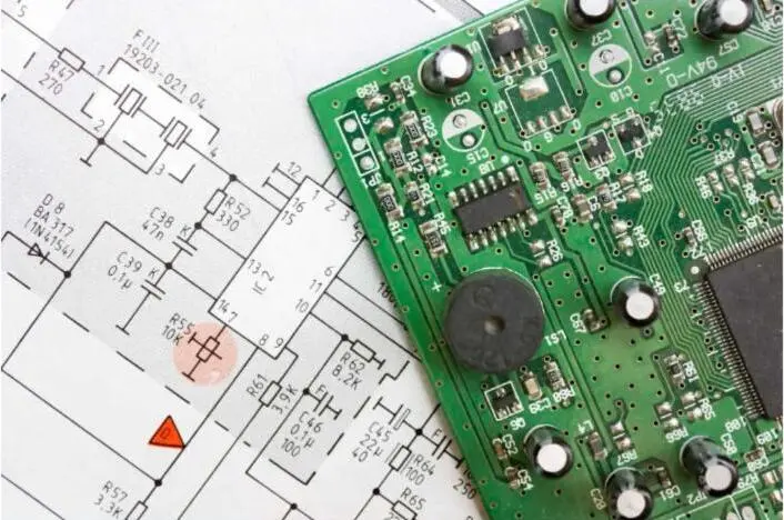
The following checklist summarizes industry-recommended rules for high-density PCBAs. These rules address probe mechanics, spacing to prevent interference and clearances that keep fixtures stable and repeatable.
- SMD test-point pad diameter should meet a preferred minimum size for reliable pogo-pin contact.
- Center-to-center test-point spacing should meet or exceed the minimum required for standard probe pitches, with larger spacing preferred to reduce adjacent probe collision.
- Test points need a minimum edge clearance so the fixture vacuum seal can grip the PCB without obstruction.
- Component clearance should meet at least the minimum requirement, with larger clearance as component height increases.
- Vias used as test points must remain untented, with hole diameter sized so the probe contacts the annular ring instead of falling into the hole.
- At least two tooling holes placed in opposite corners of the PCB are required for reliable fixture alignment.
- BGAs need dedicated test points on breakout traces or boundary-scan (JTAG) access because solder balls are inaccessible after assembly.
- When board area forces prioritization, assign test pads first to power rails and ground, then critical signals such as clocks and resets, then IC connections including BGA breakout traces, and finally passive component networks.
Managing Mechanical Stress and Board Flex
Every pogo pin applies force to the board at fixture closure. Total fixture force equals pin count multiplied by spring force per pin, and on high-density fixtures this cumulative load can be substantial. Thin or densely populated boards are especially vulnerable to flex under that load.
Boards thinner than a defined threshold require additional support points. Without those supports, flex produces open readings that disappear once the board leaves the fixture, which makes defects hard to diagnose and reproduce.
Mitigation tactics address both total load and how that load is distributed. Distribute support points under dense probe fields and heavy components to equalize load across the board. For thin or flexible boards that still deflect under mechanical pressure, vacuum hold-down fixtures reduce stress during testing. At the probe level, select pogo pins with spring forces that match pad finish and component sensitivity, and use lighter spring forces on high-density boards to limit pad lift or component stress. Keep maximum board warpage within acceptable limits to maintain reliable pogo-pin contact across the full probe field. Use pneumatic actuation to apply consistent, repeatable closure force instead of manual press-down.
BGA Access and Hybrid Test Strategies
Ball Grid Arrays create the most common testability challenge for bed-of-nails ICT because solder balls sit underneath the package and no probe reaches them after assembly. On boards with multiple high-pin-count BGAs, a significant portion of the netlist can become physically inaccessible to direct probing.
Boundary scan (IEEE 1149.1 JTAG) testing reaches coverage levels on JTAG-compliant nets that complement what bed-of-nails ICT achieves on accessible nodes. The two methods address different fault classes. ICT verifies component values, shorts, opens and polarity on probed nets. Boundary scan reports on digital interconnects through test circuitry built into the devices.
A practical decision framework for hybrid test strategy starts with the board physical accessibility. If the board has accessible test points on most nets and few BGAs, standard bed-of-nails ICT with breakout-trace test points on BGA power and ground nets can achieve adequate coverage. As BGA density increases and probe access drops, the focus shifts to which coverage gaps remain after each method, not ICT versus JTAG as a simple choice. On dense digital boards where most nets sit under BGAs, boundary scan can replace most of a bed-of-nails fixture, and a hybrid strategy retains physical test only for analog or bulk-passive measurements. X-ray inspection remains necessary for solder joints under BGAs and QFNs, because neither ICT nor boundary scan images joint geometry. Functional test remains the final gate for operational behavior that structural methods cannot verify.
For aerospace and defense applications, ICT target coverage is typically high and requires maximum test access, with every accessible net assigned a test point and JTAG likely needed for BGAs. Planning these strategies before layout freeze is the practical way to meet those targets without costly redesign.

Engage Pro-Active Engineering’s test engineering team during the design phase, before test access decisions are locked in.
Board Handling and the ICT Measurement Cycle
The ICT measurement cycle follows a defined sequence that, when executed correctly, produces repeatable and reliable results.
- Board loading: The operator or automation places the populated PCBA onto the fixture receiver and orients it against the fixture mechanical stops.
- Alignment via tooling holes: Tooling holes held to tight diameter and positional tolerances, located near opposite corners, prevent registration drift that produces intermittent failures. Guide pins engage the tooling holes and lock the board position relative to the probe field.
- Fixture closure: Pneumatic or vacuum actuation closes the fixture and presses the pogo-pin array against the test pads simultaneously. Pogo pins compress during contact while vacuum or press force applies the load.
- Signal injection: The test system applies stimulus signals, such as voltage, current or frequency, to specific nets through the probe array.
- Parametric measurement: The tester measures resistance, capacitance, inductance and other electrical parameters across the netlist, then compares results against expected values.
- Defect isolation: Out-of-tolerance measurements are flagged and logged with net-level location data, which enables targeted rework instead of board-level rejection.
- Board unloading: The fixture opens, the board is removed and the cycle repeats for the next unit.
Choosing Between ICT and Flying Probe
Bed-of-nails ICT and flying probe both perform electrical verification of board construction, but they suit different production profiles.
Bed-of-nails ICT uses a custom fixture that contacts all test points simultaneously. This approach delivers fast production because cycle times stay short once the fixture is built and the test program is validated. The tradeoff is upfront fixture development cost and lead time, along with fixture changes when the board design changes. ICT economics often favor stable, higher-volume designs.
Flying probe uses a small number of motorized probes that move across the board and contact test points one at a time. There is no custom fixture, which removes upfront tooling cost and keeps flying probe practical for prototypes, low-volume builds and boards that change often. The tradeoff is longer per-board test time, which becomes a throughput constraint at higher volumes.
For low-volume, high-mix production, boundary scan is often cheaper than ICT because it removes the custom fixture per board variant, which is the largest hidden cost of a bed-of-nails strategy. The right choice depends on volume, design stability, coverage requirements and program timeline. Pro-Active Engineering evaluates ICT, flying probe and boundary scan as part of an integrated test strategy for each program.
Frequently Asked Questions
How much coverage can ICT achieve on boards with many BGAs?
Coverage depends on how many nets have accessible test points. On boards that follow DFT rules throughout layout, ICT can achieve broad structural coverage. On boards with multiple high-pin-count BGAs and limited breakout-trace test points, coverage on those buried nets drops to near zero without supplemental methods. Boundary scan closes much of that gap for digital interconnects, and X-ray inspection addresses joint geometry under BGA packages. Boards designed for aerospace and defense programs typically target the highest coverage levels, which requires planning test access before layout is finalized. Earlier definition of test strategy preserves more options.
What drives fixture lead time and cost?
Fixture complexity is the primary driver. A board with many test points, fine probe pitch, dual-sided access or complex support requirements can take longer to design and build than a simpler single-sided fixture. Test program development, which includes writing, debugging and validating the software that runs the measurements, also affects the overall timeline. Boards that follow DFT guidelines reduce fixture complexity by keeping test points accessible, consistently sized and properly spaced, which shortens both fixture build time and test program development. Design stability before committing to ICT tooling helps control program costs because board revisions after fixture build can require fixture modifications.
When is ICT no longer viable for high-density designs?
ICT becomes difficult to justify when the board lacks enough accessible test points to achieve meaningful coverage. It also becomes less viable when probe pitch requirements exceed what the fixture technology can deliver reliably, or when the board is so densely populated that support and clearance requirements cannot be met without compromising the design. At that point, a hybrid strategy that combines flying probe, boundary scan, X-ray inspection and functional test often provides better coverage at lower risk than forcing a bed-of-nails fixture onto a design that was not built for it. The decision point is best evaluated during design review, not after assembly.
Can boundary scan fully replace physical ICT?
Boundary scan covers digital interconnects on JTAG-compliant devices, including opens, shorts, stuck-at faults and some memory faults on scan-enabled nets. It does not verify analog performance, passive component values, power rail behavior, RF paths or non-JTAG components. Physical ICT or flying probe remains necessary for those measurements. In practice, the two methods are complementary. Boundary scan closes coverage gaps on dense digital nets where probes cannot reach, and physical test handles the analog and passive measurements that boundary scan cannot address. A complete test strategy for complex PCBAs typically includes both, along with AOI, X-ray and functional test as needed.
Reduce Late-Stage Risk with an Integrated Partner
Bed-of-nails ICT delivers full value when test access, fixture mechanics and hybrid strategies are defined before layout is frozen. Decisions made at the schematic and layout stage, including test pad placement, tooling hole location, BGA breakout routing and boundary-scan chain planning, determine what coverage is achievable in production. Decisions deferred until after tape-out restrict every option that follows.

Pro-Active Engineering integrates test engineering into the design phase. The same team designs the board, plans the test strategy, builds the fixture, assembles the PCBA and runs ICT, flying probe and functional test under one roof in Sun Prairie, Wisconsin. That integration removes handoff gaps between design, assembly and test that often produce late-stage manufacturability problems on complex programs.
Pro-Active holds ISO 9001:2015, AS9100, Nadcap and JCP certifications and is ITAR-registered, which supports defense, aerospace and medical-device programs that require full traceability and disciplined documentation from design through production.
Connect with Pro-Active Engineering’s engineering team to discuss ICT feasibility, test-point strategy and integrated PCBA manufacturing for the next program.