
Last updated: August 16, 2026
Key Takeaways
- Physical probe access is the primary constraint on modern high-density PCBs, and traditional bed-of-nails fixtures alone cannot reach enough nets as BGA counts rise and board real estate shrinks.
- A coordinated test strategy that combines fixture mechanics, guarding, dual-sided probing, JTAG boundary scan and DFT rules from the first layout review closes coverage gaps on defense, aerospace and medical programs.
- Netlist-driven defect isolation, coverage reporting and early DFT test-point planning directly determine achievable ICT coverage and fixture cost on complex boards.
- Hybrid ICT + JTAG + functional test workflows deliver high structural and system-level coverage while reducing fixture complexity and lifecycle cost.
- Pro-Active Engineering delivers this integrated, ITAR-compliant workflow as a single partner. Discuss test coverage requirements for a current program.
Prerequisites: Core ICT and Test Terms
In-circuit testing (ICT): An electrical test method that contacts predefined test points on a loaded PCB to verify component presence, values, polarity, opens and shorts.
Bed-of-nails fixture: A custom mechanical fixture populated with spring-loaded pogo pins that simultaneously contact test pads across the board surface.
Guarding: A three-terminal measurement technique that drives adjacent nodes to the same potential as the measurement node, which eliminates parallel-path interference during component measurement.
Boundary scan / JTAG (IEEE 1149.1): A standard that tests interconnections through a chip’s Test Access Port (TAP) rather than through physical probes, enabling coverage of BGA solder joints and buried digital nets.
Flying probe: A fixtureless test method using motorized probes that contact test points sequentially, suited for low-volume or early-prototype boards where fixture investment is not yet justified.
Functional test (FCT): A powered test that verifies end-to-end system behavior against the product specification and complements ICT’s component-level coverage.
Step 1: Aligning Bed-of-Nails Fixtures to the PCB
A bed-of-nails fixture is a custom-machined plate drilled to match the test-point coordinates of a specific board variant. Spring-loaded pogo pins press into each hole and connect to the ICT system’s measurement channels.
Alignment accuracy sets the ceiling for contact reliability. Tooling holes and adequate separation between test pads improve fixture alignment and increase coverage on finished boards. Fiducials on the PCB provide optical registration references that keep the fixture repeatable across production shifts.

Spring-loaded test pins deliver reliable contact only within a defined force window per pin. Excessive force risks pad cratering or board flex, while low force produces high-resistance readings. Fixture design must account for board thickness, component height clearances and the mix of pin styles required for a given layout.
For double-sided SMT assemblies, a clamshell fixture configuration contacts both board surfaces simultaneously. This dual-sided approach connects directly to the probing strategies described in Step 3.
Review fixture requirements for a specific board design.
Step 2: Guarding Techniques for Parallel Circuits
Parallel paths on dense interconnected boards distort standard two-terminal measurements. A two-terminal setup reads the equivalent of all parallel paths at once rather than the target component alone, which can produce false failures or false passes.
ICT guarding resolves this with a three-terminal approach that eliminates parallel-path interference. The tester drives adjacent leakage nodes to the same potential as the measurement node, which removes the voltage difference across those paths. With no current flowing through the parallel circuits, the instrument measures only the target component.
Individual responses for resistors, capacitors, inductors, diodes and polarized capacitors can be masked by parallel paths when guarding is absent or configured poorly. This measurement challenge is why precision guarding capability differentiates enterprise-grade ICT platforms from lower-tier alternatives that lack the channel count or switching performance to support it.
Guarding delivers the greatest value on analog-heavy boards where high-value passives sit near low-impedance power distribution networks. The technique isolates components embedded deep within complex schematics and preserves defect visibility.
Plan analog coverage for a dense board design.
Step 3: Dual-Sided and Bi-Level Probing on Dense Assemblies
Dual-sided probing restores access on double-sided SMT assemblies that single-sided fixtures cannot reach. Dual-sided fixtures probe top and bottom surfaces simultaneously using a clamshell or vacuum-actuated clamp configuration.
Bi-level probing extends this access by mixing pin heights within a single fixture plate. Taller pins reach test points near the board center, while shorter pins contact pads near the edges. This structure supports boards with varied component heights and keepout zones.
Double-sided assembly with limited access can reduce ICT coverage to the point where neither ICT nor flying probe alone is sufficient. Dual-sided fixture design, combined with early DFT planning, recovers a meaningful portion of that coverage before JTAG or flying probe fallback becomes necessary.
Fixture cost for dual-sided configurations exceeds single-sided equivalents. That investment pays off when board complexity and production volume make test escapes more expensive than the fixture itself.
Evaluate dual-sided fixture options for a current layout.
Step 4: Integrating JTAG Boundary Scan for Inaccessible Nodes
BGA solder joints sit beneath the package body and remain physically unreachable by probes. Boundary scan verifies BGA solder joints for opens and shorts using boundary-scan cells that drive and sense every pin via the four-wire JTAG port, which uses TDI, TDO, TCK and TMS routed to an accessible connector or test pad.

IEEE 1149.1 boundary scan was adopted to address the loss of physical access caused by fine-pitch components and BGA devices that made traditional bed-of-nails fixtures more expensive and less reliable. The standard inserts boundary-scan cells on each I/O pin and chains them into a shift register, which enables interconnect testing without direct probe contact.
A hybrid ICT + JTAG strategy fits dense digital boards. Boundary scan handles digital interconnect, BGA joints and flash programming while physical probing covers analog and bulk-passive measurements that require direct contact.
Board readiness for boundary scan depends on scan device density, chain integrity, verified BSDL files for every scan device and JTAG signal integrity, including buffering on TCK and TMS lines. Early DFT planning that defines how boundary scan complements ICT allows designers to reduce fixture complexity and cost while improving defect isolation for inaccessible nodes.
Integrate JTAG boundary scan into a test strategy for a BGA-heavy design.
Step 5: Using Netlists for Defect Isolation and Coverage Reporting
ICT test programs derive from the board netlist, which defines every electrical connection. Each net in the netlist becomes a test target, and the program drives stimulus, measures response and compares results against tolerance limits derived from known-good board data.
Netlist completeness directly determines coverage because each defined net can receive a test. Boards designed without adequate test-point coverage cannot achieve full ICT coverage regardless of fixture quality, which means this constraint must be addressed during schematic and layout rather than after the board is built.
Coverage reporting quantifies results by fault class, including opens, shorts, wrong-value components and wrong polarity, and maps each fault to a specific net. Coverage reports guide fixture investment decisions and show where JTAG boundary scan is sufficient versus where physical fixtures add value. The coverage gaps these reports reveal become preventable when test requirements feed into design.
Review netlist completeness and coverage targets for a program.
Step 6: DFT Test-Point and Netlist Requirements in Layout
DFT rules for ICT must be established before layout is finalized. In-circuit testability must be considered during PCB design rather than after routing to prevent coverage loss and fixture compromises on dense boards.
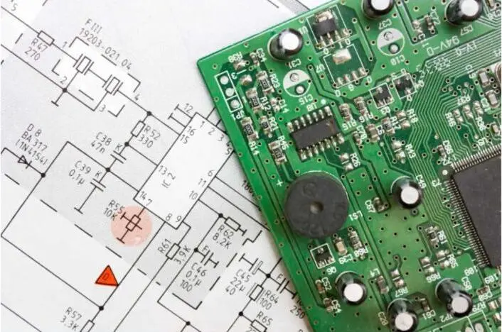
The following layout requirements directly determine whether a board can achieve the probe access and netlist coverage that ICT depends on:
- Test point pad diameters meeting minimum probe contact requirements for standard or fine-pitch probes
- Round exposed pads on critical nets including power rails, ground, reset, clocks and communication signals
- Single-side test point placement where possible to reduce fixture cost and complexity
- Adequate center-to-center probe pitch spacing between adjacent test points
- Tooling holes and fiducials positioned per the fixture alignment requirements established in Step 1
- At least one test point per net in the netlist
- Avoidance of test point placement under component bodies
Via-in-pad or short breakout stubs on BGA power and ground nets recover additional ICT coverage that would otherwise remain inaccessible on multilayer boards.
For JTAG integration, PCB layout must include JTAG headers or accessible test pads, reserved fixture space and documented chain order. BSDL files for every scan device must be verified before test program generation.
Pro-Active Engineering integrates DFM and DFT review into the design phase, catching access gaps before layout freeze rather than after first article build.
Schedule a DFT review for an upcoming board design.
Step 7: Combining ICT with Functional Test for Full Coverage
ICT verifies structural integrity at the component level and confirms that parts are present, correctly valued and properly connected. It does not verify firmware behavior, signal integrity, system timing or end-to-end functional performance.
ICT is strongest on opens, shorts and component-value defects but cannot detect functional behavior, firmware-related failures or system-level timing. Functional test addresses that gap by powering the full assembly and exercising it against the product specification.
A hybrid ICT + functional test strategy fits boards that include programmable devices, tight signal integrity margins or regulatory requirements for documented functional verification. It also supports programs where field failure modes include latent defects that structural test alone cannot reveal.
Pro-Active Engineering designs and builds custom functional test systems as part of its integrated workflow, which extends coverage from component-level ICT through full system validation without involving a separate test vendor.
Plan functional test alongside ICT for a current program.
Supporting Frameworks and Common Implementation Challenges
The seven steps above describe the technical workflow for ICT coverage. Effective ICT programs also rely on structured frameworks that identify risks and prevent common implementation mistakes.
Process Failure Mode and Effects Analysis (PFMEA) identifies fault classes with the highest risk and informs coverage priorities. DFM checklists applied during layout review catch test-point omissions, spacing violations and netlist gaps before they become fixture problems. IPC workmanship standards, including IPC-A-610, establish the quality baseline used to interpret ICT results.
Common challenges and mitigations include:
- Incomplete netlists: Test programs generated from partial netlists produce incomplete coverage maps. Mitigation requires a complete, verified netlist before test program development begins.
- Late test-point additions: The most common DFT mistake is treating testability as an afterthought. Test points added after layout freeze often conflict with component placement or routing, which reduces their effectiveness. Early cross-functional DFT review prevents this issue.
- Fixture cost justification: Bed-of-nails fixtures involve non-recurring engineering costs for machining, wiring and debugging. For lower volumes, a hybrid flying-probe and JTAG strategy reduces upfront fixture investment while maintaining structural coverage.
Discuss DFT framework requirements for a specific program phase.
Evaluating Test Strategy Effectiveness: Key Performance Indicators
Once the ICT workflow is implemented, test strategy effectiveness is measured against production outcomes rather than coverage percentages alone. The following indicators track whether the test program delivers the defect isolation and yield improvements it targets.
- First-pass yield (FPY): The percentage of boards passing ICT without rework. DFT-compliant layouts consistently achieve higher first-pass ICT yields compared with designs that omit test-point planning.
- Defect escape rate: The number of defective boards reaching downstream test stages or the field. Lower escape rates indicate that ICT and JTAG coverage catch faults at the earliest, least costly stage.
- Fault isolation time: The time required to diagnose a failing board. Netlist-driven coverage reports and boundary-scan diagnostics reduce isolation time compared with manual debug.
- On-time delivery: Test cycle efficiency, including fixture changeover and program execution time, directly affects production throughput and delivery predictability.
Pro-Active Engineering tracks these metrics across the production lifecycle and uses them to improve fixture design, test program quality and DFT guidance for future programs.
Set test coverage and yield targets for an upcoming build.
Frequently Asked Questions
What is the difference between ICT and functional testing, and does a program need both?
The distinction outlined in Step 7 centers on scope. ICT catches manufacturing defects at the component level, while functional testing validates system behavior under power. Most defense, aerospace and medical programs benefit from both, with ICT running first to remove structural defects before functional test begins. Pro-Active Engineering designs and builds custom functional test systems as part of its integrated workflow.
How does JTAG boundary scan improve coverage on BGA-heavy boards?
As described in Step 4, JTAG boundary scan addresses the BGA access problem by testing interconnections through the chip’s Test Access Port rather than through physical probes. The technique is most effective when combined with bed-of-nails ICT for analog and passive coverage, which creates a hybrid strategy that reaches both accessible and inaccessible nodes.
When should a program use flying probe instead of a bed-of-nails fixture?
Flying probe is a fixtureless test method that contacts test points sequentially using motorized probes. It removes the non-recurring engineering cost of a custom fixture, which suits low-volume builds, early prototypes and high-mix production where board variants change frequently. The tradeoff is test cycle time because flying probe tests boards sequentially rather than simultaneously, which reduces throughput compared with a bed-of-nails fixture. For programs with higher volumes and stable board designs, bed-of-nails fixtures recover that throughput and repay their upfront cost. Pro-Active Engineering evaluates both approaches based on program volume, board complexity and coverage requirements.
What ITAR and compliance considerations apply to PCB test programs?
Defense and aerospace programs subject to ITAR require that test data, netlists, firmware and board documentation remain within a controlled ITAR-registered facility. Test programs for controlled assemblies must be generated, stored and executed under access controls that restrict foreign-national exposure per DDTC requirements. Pro-Active Engineering is ITAR-registered and applies documented data-handling procedures, personnel training records and access controls across its engineering and manufacturing workflow. Programs also benefit from Pro-Active’s AS9100 certification, Nadcap accreditation and JCP certification, which establish the quality and traceability framework that regulated programs require.

How early in the design process should DFT planning begin?
DFT planning should begin at schematic capture, before PCB layout starts. Test-point placement, JTAG chain architecture, netlist completeness and fixture access zones are all constrained by routing and component placement decisions made during layout. Changes to test-point locations after layout freeze often conflict with existing routing or component keepouts, which reduces their effectiveness and can require a board respin. Pro-Active Engineering integrates DFT review into the design phase as part of its DFM workflow, identifying access gaps and coverage risks before layout is finalized. This approach reduces fixture cost, shortens test program development time and improves first-pass yield from the first production build.
Conclusion: Partner with Pro-Active Engineering
Limited probe access on complex PCBs becomes manageable when fixture mechanics, guarding, dual-sided probing, JTAG boundary scan and DFT rules align from the first design review. Each step in this workflow builds on the previous one, and gaps at any stage reduce coverage and raise lifecycle cost.
Pro-Active Engineering delivers this integrated workflow as a single ITAR-compliant partner. From DFM-driven PCB design and rapid prototyping through ICT, JTAG, flying-probe and functional test in production, every stage operates within one accountable engineering and manufacturing system. Defense, aerospace and medical programs gain full traceability, certified quality management and a domestic supply chain built for mission-critical reliability.
Pro-Active Engineering’s team collaborates on test-coverage requirements, fixture strategy and DFT review for active programs.
Start a test strategy discussion with the engineering team.